
AMD Xilinx
XC2V80-6CS144C
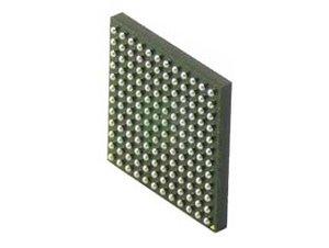
XC2V80-6CS144C ECAD Model
XC2V80-6CS144C Attributes
| Type | Description | Select |
|---|---|---|
| Pbfree Code | No | |
| Rohs Code | No | |
| Part Life Cycle Code | Obsolete | |
| Supply Voltage-Nom | 1.5 V | |
| Number of Inputs | 92 | |
| Number of Outputs | 92 | |
| Number of Logic Cells | 1152 | |
| Number of Equivalent Gates | 80000 | |
| Number of CLBs | 128 | |
| Combinatorial Delay of a CLB-Max | 350 ps | |
| Programmable Logic Type | FIELD PROGRAMMABLE GATE ARRAY | |
| Temperature Grade | OTHER | |
| Package Shape | SQUARE | |
| Technology | CMOS | |
| Organization | 128 CLBS, 80000 GATES | |
| Clock Frequency-Max | 820 MHz | |
| Power Supplies | 1.5,1.5/3.3,3.3 V | |
| Supply Voltage-Max | 1.575 V | |
| Supply Voltage-Min | 1.425 V | |
| JESD-30 Code | S-PBGA-B144 | |
| Qualification Status | Not Qualified | |
| JESD-609 Code | e0 | |
| Moisture Sensitivity Level | 3 | |
| Operating Temperature-Max | 85 °C | |
| Peak Reflow Temperature (Cel) | 240 | |
| Time@Peak Reflow Temperature-Max (s) | 30 | |
| Number of Terminals | 144 | |
| Package Body Material | PLASTIC/EPOXY | |
| Package Code | TFBGA | |
| Package Equivalence Code | BGA144,13X13,32 | |
| Package Shape | SQUARE | |
| Package Style | GRID ARRAY, THIN PROFILE, FINE PITCH | |
| Surface Mount | YES | |
| Terminal Finish | Tin/Lead (Sn63Pb37) | |
| Terminal Form | BALL | |
| Terminal Pitch | 800 µm | |
| Terminal Position | BOTTOM | |
| Width | 12 mm | |
| Length | 12 mm | |
| Seated Height-Max | 1.2 mm | |
| Ihs Manufacturer | XILINX INC | |
| Part Package Code | BGA | |
| Package Description | 12 X 12 MM, 0.80 MM PITCH, MO-216BAG-2, CSP-144 | |
| Pin Count | 144 | |
| Reach Compliance Code | not_compliant | |
| ECCN Code | EAR99 | |
| HTS Code | 8542.39.00.01 |
XC2V80-6CS144C Datasheet Download
XC2V80-6CS144C Overview
XC2V80-6CS144C is a chip model developed by Xilinx Inc., a leader in the field of programmable logic devices. It is a field-programmable gate array (FPGA) device that is widely used in high-performance digital signal processing, embedded processing, and image processing applications. It is designed to be programmed with a hardware description language (HDL) such as VHDL or Verilog.
The XC2V80-6CS144C chip model was designed with the intention of providing a powerful and flexible solution for a variety of applications. Its features include a high-speed 6-input look-up table (LUT) architecture, a high-speed embedded RAM block, and a high-speed DSP block. It also has the capability for future upgrades, including the ability to add additional logic blocks and memory blocks. This makes it an ideal solution for high-performance applications such as advanced communication systems.
The XC2V80-6CS144C chip model is also suitable for the development and popularization of future intelligent robots. Its high-speed processing and embedded RAM blocks are ideal for applications such as robotic vision and motion control. To use the model effectively, technical talents such as engineers and computer scientists are needed to design and implement the necessary HDL code.
In conclusion, the XC2V80-6CS144C chip model is a powerful and flexible solution for a variety of applications. It is suitable for high-performance digital signal processing, embedded processing, image processing, and advanced communication systems. It is also suitable for the development and popularization of future intelligent robots. To use the model effectively, technical talents such as engineers and computer scientists are needed to design and implement the necessary HDL code.
You May Also Be Interested In
4,511 In Stock
Pricing (USD)
| QTY | Unit Price | Ext Price |
|---|---|---|
| No reference price found. | ||