
AMD Xilinx
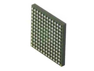
XC2V250-5CS144C
XC2V250-5CS144C ECAD Model
XC2V250-5CS144C Attributes
| Type | Description | Select |
|---|---|---|
| Pbfree Code | No | |
| Rohs Code | No | |
| Part Life Cycle Code | Obsolete | |
| Supply Voltage-Nom | 1.5 V | |
| Number of Inputs | 92 | |
| Number of Outputs | 92 | |
| Number of Logic Cells | 3456 | |
| Number of Equivalent Gates | 250000 | |
| Number of CLBs | 384 | |
| Combinatorial Delay of a CLB-Max | 390 ps | |
| Programmable Logic Type | FIELD PROGRAMMABLE GATE ARRAY | |
| Temperature Grade | OTHER | |
| Package Shape | SQUARE | |
| Technology | CMOS | |
| Organization | 384 CLBS, 250000 GATES | |
| Clock Frequency-Max | 750 MHz | |
| Power Supplies | 1.5,1.5/3.3,3.3 V | |
| Supply Voltage-Max | 1.575 V | |
| Supply Voltage-Min | 1.425 V | |
| JESD-30 Code | S-PBGA-B144 | |
| Qualification Status | Not Qualified | |
| JESD-609 Code | e0 | |
| Moisture Sensitivity Level | 3 | |
| Operating Temperature-Max | 85 °C | |
| Peak Reflow Temperature (Cel) | 240 | |
| Time@Peak Reflow Temperature-Max (s) | 30 | |
| Number of Terminals | 144 | |
| Package Body Material | PLASTIC/EPOXY | |
| Package Code | TFBGA | |
| Package Equivalence Code | BGA144,13X13,32 | |
| Package Shape | SQUARE | |
| Package Style | GRID ARRAY, THIN PROFILE, FINE PITCH | |
| Surface Mount | YES | |
| Terminal Finish | Tin/Lead (Sn63Pb37) | |
| Terminal Form | BALL | |
| Terminal Pitch | 800 µm | |
| Terminal Position | BOTTOM | |
| Width | 12 mm | |
| Length | 12 mm | |
| Seated Height-Max | 1.2 mm | |
| Ihs Manufacturer | XILINX INC | |
| Part Package Code | BGA | |
| Package Description | 12 X 12 MM, 0.80 MM PITCH, MO-216BAG-2, CSP-144 | |
| Pin Count | 144 | |
| Reach Compliance Code | not_compliant | |
| HTS Code | 8542.39.00.01 | |
| ECCN Code | EAR99 |
XC2V250-5CS144C Datasheet Download
XC2V250-5CS144C Overview
XC2V250-5CS144C is a powerful and versatile chip model designed by Xilinx for a wide range of applications. It is a Field-Programmable Gate Array (FPGA) with a Virtex-II Pro platform. This chip model has a capacity of up to 250K logic cells, 5 million system gates, and 144 I/O pins.
The advantages of XC2V250-5CS144C include its high-speed performance, low-power consumption, and high-density integration. It has a wide range of features that make it suitable for a variety of applications, including high-speed signal processing, image processing, and embedded systems. It also offers a high level of flexibility and scalability, making it possible to customize the design to meet specific requirements.
The expected demand trends for the XC2V250-5CS144C in related industries are expected to be strong in the coming years. With its high-speed performance and low-power consumption, it is ideal for use in the 5G mobile communication systems and the Internet of Things (IoT). It is also expected to be used in automotive applications, such as autonomous driving and in-vehicle infotainment.
The original design intention of the XC2V250-5CS144C was to provide a powerful, yet low-cost solution for a wide range of applications. It is designed to be highly scalable and customizable, allowing for future upgrades and modifications to meet changing needs.
The XC2V250-5CS144C can be used in advanced communication systems, such as 5G mobile communication systems and the Internet of Things (IoT). It can also be used in other applications, such as high-speed signal processing, image processing, and embedded systems.
The product description and specific design requirements of the XC2V250-5CS144C are detailed in the user manual. It is important to read and understand the user manual in order to properly configure and use the chip model. Additionally, it is important to consider the actual use case when designing the chip model, as the design must be tailored to the specific application.
Case studies have been conducted on the XC2V250-5CS144C to demonstrate its effectiveness in various applications. For example, in a 5G mobile communication system, the chip model was used to handle the high-speed data processing requirements. In an autonomous driving application, the chip model was used to process the high-resolution images from the vehicle’s sensors.
When using the XC2V250-5CS144C, it is important to consider the power requirements of the application and the chip model. Additionally, it is important to ensure that the design is optimized for the specific application in order to maximize the performance of the chip model.
In conclusion, the XC2V250-5CS144C is a powerful and versatile chip model designed by Xilinx for a wide range of applications. It has a wide range of features that make it suitable for a variety of applications, including high-speed signal processing, image processing, and embedded systems. The expected demand trends for the chip model in related industries are expected to be strong in the coming years. It is important to read and understand the user manual in order to properly configure and use the chip model, and to consider the actual use case when designing the chip model. Additionally, it is important to consider the power requirements of the application and the chip model, and to ensure that the design is optimized for the specific application in order to maximize the performance of the chip model.
You May Also Be Interested In
3,914 In Stock
Pricing (USD)
| QTY | Unit Price | Ext Price |
|---|---|---|
| No reference price found. | ||