
AMD Xilinx
XC2V8000-6FFG1517C
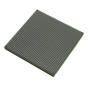
XC2V8000-6FFG1517C ECAD Model
XC2V8000-6FFG1517C Attributes
| Type | Description | Select |
|---|---|---|
| Pbfree Code | Yes | |
| Rohs Code | Yes | |
| Part Life Cycle Code | Obsolete | |
| Supply Voltage-Nom | 1.5 V | |
| Number of Equivalent Gates | 8000000 | |
| Number of CLBs | 11648 | |
| Combinatorial Delay of a CLB-Max | 350 ps | |
| Programmable Logic Type | FIELD PROGRAMMABLE GATE ARRAY | |
| Temperature Grade | OTHER | |
| Package Shape | SQUARE | |
| Technology | CMOS | |
| Organization | 11648 CLBS, 8000000 GATES | |
| Clock Frequency-Max | 820 MHz | |
| Supply Voltage-Max | 1.575 V | |
| Supply Voltage-Min | 1.425 V | |
| JESD-30 Code | S-PBGA-B1517 | |
| Qualification Status | Not Qualified | |
| JESD-609 Code | e1 | |
| Moisture Sensitivity Level | 4 | |
| Operating Temperature-Max | 85 °C | |
| Peak Reflow Temperature (Cel) | 245 | |
| Time@Peak Reflow Temperature-Max (s) | 30 | |
| Number of Terminals | 1517 | |
| Package Body Material | PLASTIC/EPOXY | |
| Package Code | BGA | |
| Package Shape | SQUARE | |
| Package Style | GRID ARRAY | |
| Surface Mount | YES | |
| Terminal Finish | Tin/Silver/Copper (Sn95.5Ag4.0Cu0.5) | |
| Terminal Form | BALL | |
| Terminal Pitch | 1 mm | |
| Terminal Position | BOTTOM | |
| Width | 40 mm | |
| Length | 40 mm | |
| Seated Height-Max | 3.4 mm | |
| Ihs Manufacturer | XILINX INC | |
| Part Package Code | BGA | |
| Package Description | 40 X 40 MM, 1 MM PITCH, MS-034AAU-1, FLIP CHIP, FBGA-1517 | |
| Pin Count | 1517 | |
| Reach Compliance Code | not_compliant | |
| HTS Code | 8542.39.00.01 |
XC2V8000-6FFG1517C Datasheet Download
XC2V8000-6FFG1517C Overview
The XC2V8000-6FFG1517C chip model is a high-performance field programmable gate array (FPGA) developed by Xilinx. It is designed with a Virtex-II Pro FPGA core and features a wide range of features that make it suitable for a variety of high-performance applications. It is particularly well-suited for digital signal processing, embedded processing, image processing, and other demanding tasks.
The XC2V8000-6FFG1517C chip model is a powerful tool for engineers, developers, and researchers, as it offers the flexibility to quickly design, test, and deploy complex systems. It also provides a wide range of features that make it suitable for a variety of applications, such as high-performance digital signal processing, embedded processing, image processing, and more. The chip model requires the use of a hardware description language (HDL) such as Verilog or VHDL to program and configure the FPGA.
The XC2V8000-6FFG1517C chip model offers a number of advantages over other FPGA models, including high-speed operation, low power consumption, and a wide range of features. As a result, the demand for this chip model is expected to increase in the near future as more applications require high-performance FPGA solutions.
The XC2V8000-6FFG1517C chip model can be used in the development and popularization of future intelligent robots, as it offers the flexibility to quickly design, test, and deploy complex systems. However, it requires a certain level of technical expertise to use the model effectively. Those who wish to use the XC2V8000-6FFG1517C chip model should be familiar with HDL programming, as well as have a good understanding of digital signal processing, embedded processing, and image processing. Additionally, they should have a good knowledge of the FPGA architecture and be able to work with the Xilinx tools.
You May Also Be Interested In
5,961 In Stock
Pricing (USD)
| QTY | Unit Price | Ext Price |
|---|---|---|
| No reference price found. | ||