
AMD Xilinx
XC2V8000-6FF1517I
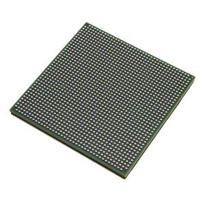
XC2V8000-6FF1517I ECAD Model
XC2V8000-6FF1517I Attributes
| Type | Description | Select |
|---|---|---|
| Pbfree Code | No | |
| Rohs Code | No | |
| Part Life Cycle Code | Obsolete | |
| Supply Voltage-Nom | 1.5 V | |
| Number of Inputs | 1108 | |
| Number of Outputs | 1108 | |
| Number of Logic Cells | 104832 | |
| Number of Equivalent Gates | 8000000 | |
| Number of CLBs | 11648 | |
| Combinatorial Delay of a CLB-Max | 350 ps | |
| Programmable Logic Type | FIELD PROGRAMMABLE GATE ARRAY | |
| Package Shape | SQUARE | |
| Technology | CMOS | |
| Organization | 11648 CLBS, 8000000 GATES | |
| Clock Frequency-Max | 820 MHz | |
| Power Supplies | 1.5,1.5/3.3,3.3 V | |
| Supply Voltage-Max | 1.575 V | |
| Supply Voltage-Min | 1.425 V | |
| JESD-30 Code | S-PBGA-B1517 | |
| Qualification Status | Not Qualified | |
| JESD-609 Code | e0 | |
| Moisture Sensitivity Level | 4 | |
| Peak Reflow Temperature (Cel) | 225 | |
| Time@Peak Reflow Temperature-Max (s) | 30 | |
| Number of Terminals | 1517 | |
| Package Body Material | PLASTIC/EPOXY | |
| Package Code | BGA | |
| Package Equivalence Code | BGA1517,39X39,40 | |
| Package Shape | SQUARE | |
| Package Style | GRID ARRAY | |
| Surface Mount | YES | |
| Terminal Finish | Tin/Lead (Sn63Pb37) | |
| Terminal Form | BALL | |
| Terminal Pitch | 1 mm | |
| Terminal Position | BOTTOM | |
| Width | 40 mm | |
| Length | 40 mm | |
| Seated Height-Max | 3.4 mm | |
| Ihs Manufacturer | XILINX INC | |
| Part Package Code | BGA | |
| Package Description | 40 X 40 MM, 1 MM PITCH, MS-034AAU-1, FLIP CHIP, FBGA-1517 | |
| Pin Count | 1517 | |
| Reach Compliance Code | not_compliant | |
| HTS Code | 8542.39.00.01 |
XC2V8000-6FF1517I Datasheet Download
XC2V8000-6FF1517I Overview
The XC2V8000-6FF1517I is a high-performance field-programmable gate array (FPGA) designed for digital signal processing, embedded processing, and image processing. It is one of the most advanced FPGA models available today, and its features make it an ideal choice for a wide range of applications.
The XC2V8000-6FF1517I is capable of delivering a high level of performance while consuming minimal power. It is also highly configurable, allowing users to customize the device to their specific needs. This makes it well-suited for applications such as medical imaging, video surveillance, and machine vision. Furthermore, its support for the HDL language makes it suitable for a variety of projects.
The XC2V8000-6FF1517I has been designed with the intention of providing users with an efficient and reliable platform for their projects. It is capable of handling a wide range of tasks, from basic signal processing to more complex embedded processing. Furthermore, its ability to be upgraded makes it an attractive choice for those looking to future-proof their projects.
The XC2V8000-6FF1517I is also suitable for advanced communication systems. Its high-speed signal processing capabilities allow it to handle high-bandwidth data streams with ease, making it an ideal choice for applications such as 5G networks. Furthermore, its low power consumption makes it an attractive choice for battery-powered devices.
The XC2V8000-6FF1517I has seen increasing demand in recent years, and this trend is expected to continue in the future. Its wide range of features make it an attractive choice for a variety of applications, and its ability to be upgraded makes it a good choice for those looking to future-proof their projects. As such, the XC2V8000-6FF1517I is an ideal choice for those looking for a reliable and efficient FPGA.
You May Also Be Interested In
5,787 In Stock
Pricing (USD)
| QTY | Unit Price | Ext Price |
|---|---|---|
| No reference price found. | ||