AMD Xilinx
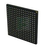
XC2V80-5FG256C
XC2V80-5FG256C ECAD Model
XC2V80-5FG256C Attributes
| Type | Description | Select |
|---|---|---|
| Pbfree Code | No | |
| Rohs Code | No | |
| Part Life Cycle Code | Obsolete | |
| Supply Voltage-Nom | 1.5 V | |
| Number of Inputs | 120 | |
| Number of Outputs | 120 | |
| Number of Logic Cells | 1152 | |
| Number of Equivalent Gates | 80000 | |
| Number of CLBs | 128 | |
| Combinatorial Delay of a CLB-Max | 390 ps | |
| Programmable Logic Type | FIELD PROGRAMMABLE GATE ARRAY | |
| Temperature Grade | OTHER | |
| Package Shape | SQUARE | |
| Technology | CMOS | |
| Organization | 128 CLBS, 80000 GATES | |
| Clock Frequency-Max | 750 MHz | |
| Power Supplies | 1.5,1.5/3.3,3.3 V | |
| Supply Voltage-Max | 1.575 V | |
| Supply Voltage-Min | 1.425 V | |
| JESD-30 Code | S-PBGA-B256 | |
| Qualification Status | Not Qualified | |
| JESD-609 Code | e0 | |
| Moisture Sensitivity Level | 3 | |
| Operating Temperature-Max | 85 °C | |
| Peak Reflow Temperature (Cel) | 225 | |
| Time@Peak Reflow Temperature-Max (s) | 30 | |
| Number of Terminals | 256 | |
| Package Body Material | PLASTIC/EPOXY | |
| Package Code | BGA | |
| Package Equivalence Code | BGA256,16X16,40 | |
| Package Shape | SQUARE | |
| Package Style | GRID ARRAY | |
| Surface Mount | YES | |
| Terminal Finish | Tin/Lead (Sn63Pb37) | |
| Terminal Form | BALL | |
| Terminal Pitch | 1 mm | |
| Terminal Position | BOTTOM | |
| Width | 17 mm | |
| Length | 17 mm | |
| Seated Height-Max | 2 mm | |
| Ihs Manufacturer | XILINX INC | |
| Part Package Code | BGA | |
| Package Description | 17 X 17 MM, 1 MM PITCH, MO-034AAF-1, FBGA-256 | |
| Pin Count | 256 | |
| Reach Compliance Code | not_compliant | |
| ECCN Code | EAR99 | |
| HTS Code | 8542.39.00.01 |
XC2V80-5FG256C Datasheet Download
XC2V80-5FG256C Overview
The chip model XC2V80-5FG256C is a programmable logic device (PLD) from Xilinx, a leading provider of programmable logic solutions. This chip model is designed for high-end applications that require high performance, low power consumption, and flexibility. It is a field-programmable gate array (FPGA) that can be easily configured to meet specific design requirements.
The XC2V80-5FG256C chip offers a number of advantages, including a high speed, low power consumption, and flexibility. It features a high-speed, low-power Virtex-2V FPGA core, 256Kbits of block RAM, and up to 1.5Mbits of distributed RAM. The chip also includes a large number of user-programmable I/Os and a wide range of dedicated peripherals. This makes it suitable for a variety of applications, including automotive, industrial, medical, and consumer electronics.
In terms of industry trends, the XC2V80-5FG256C chip is expected to experience a surge in demand in the coming years. This is due to the increasing demand for advanced technology in various industries, such as automotive, industrial, medical, and consumer electronics. The chip is also expected to benefit from the growing demand for FPGAs in the market, as they offer more flexibility and performance than traditional ASICs.
In terms of product description, the XC2V80-5FG256C chip is designed for high-end applications that require high performance and low power consumption. It features a high-speed, low-power Virtex-2V FPGA core, 256Kbits of block RAM, and up to 1.5Mbits of distributed RAM. The chip also includes a large number of user-programmable I/Os and a wide range of dedicated peripherals. This makes it suitable for a variety of applications, including automotive, industrial, medical, and consumer electronics.
In terms of design requirements, the XC2V80-5FG256C chip requires a specific set of design parameters, such as the number of logic blocks, the number of I/Os, and the type of memory. Additionally, the chip must be configured to meet the specific design requirements of the application.
In terms of actual case studies, there are a number of examples of successful applications of the XC2V80-5FG256C chip. For example, the chip has been used in a variety of automotive applications, such as vehicle control systems and navigation systems. Additionally, the chip has been used in medical applications, such as patient monitoring systems and medical imaging systems.
Finally, in terms of precautions, the XC2V80-5FG256C chip must be designed and configured carefully to meet the specific requirements of the application. Additionally, the chip must be tested thoroughly to ensure that it is functioning properly.
In conclusion, the XC2V80-5FG256C chip is a highly advanced and flexible FPGA that is expected to experience a surge in demand in the coming years. It is designed for high-end applications that require high performance and low power consumption. Additionally, it requires a specific set of design parameters and must be tested thoroughly to ensure that it is functioning properly. Finally, there are a number of successful case studies of the chip being used in various applications, such as automotive, industrial, medical, and consumer electronics.
You May Also Be Interested In
5,541 In Stock
Pricing (USD)
| QTY | Unit Price | Ext Price |
|---|---|---|
| 1+ | $63.6120 | $63.6120 |
| 10+ | $62.9280 | $629.2800 |
| 100+ | $59.5080 | $5,950.8000 |
| 1000+ | $56.0880 | $28,044.0000 |
| 10000+ | $51.3000 | $51,300.0000 |
| The price is for reference only, please refer to the actual quotation! | ||
