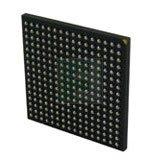
AMD Xilinx
XC2V500-6FG256C
XC2V500-6FG256C ECAD Model
XC2V500-6FG256C Attributes
| Type | Description | Select |
|---|---|---|
| Pbfree Code | No | |
| Rohs Code | No | |
| Part Life Cycle Code | Obsolete | |
| Supply Voltage-Nom | 1.5 V | |
| Number of Inputs | 172 | |
| Number of Outputs | 172 | |
| Number of Logic Cells | 6912 | |
| Number of Equivalent Gates | 500000 | |
| Number of CLBs | 768 | |
| Combinatorial Delay of a CLB-Max | 350 ps | |
| Programmable Logic Type | FIELD PROGRAMMABLE GATE ARRAY | |
| Temperature Grade | OTHER | |
| Package Shape | SQUARE | |
| Technology | CMOS | |
| Organization | 768 CLBS, 500000 GATES | |
| Clock Frequency-Max | 820 MHz | |
| Power Supplies | 1.5,1.5/3.3,3.3 V | |
| Supply Voltage-Max | 1.575 V | |
| Supply Voltage-Min | 1.425 V | |
| JESD-30 Code | S-PBGA-B256 | |
| Qualification Status | Not Qualified | |
| JESD-609 Code | e0 | |
| Moisture Sensitivity Level | 3 | |
| Operating Temperature-Max | 85 °C | |
| Peak Reflow Temperature (Cel) | 225 | |
| Time@Peak Reflow Temperature-Max (s) | 30 | |
| Number of Terminals | 256 | |
| Package Body Material | PLASTIC/EPOXY | |
| Package Code | BGA | |
| Package Equivalence Code | BGA256,16X16,40 | |
| Package Shape | SQUARE | |
| Package Style | GRID ARRAY | |
| Surface Mount | YES | |
| Terminal Finish | Tin/Lead (Sn63Pb37) | |
| Terminal Form | BALL | |
| Terminal Pitch | 1 mm | |
| Terminal Position | BOTTOM | |
| Width | 17 mm | |
| Length | 17 mm | |
| Seated Height-Max | 2 mm | |
| Ihs Manufacturer | XILINX INC | |
| Part Package Code | BGA | |
| Package Description | 17 X 17 MM, 1 MM PITCH, MO-034AAF-1, FBGA-256 | |
| Pin Count | 256 | |
| Reach Compliance Code | not_compliant | |
| ECCN Code | EAR99 | |
| HTS Code | 8542.39.00.01 |
XC2V500-6FG256C Datasheet Download
XC2V500-6FG256C Overview
The XC2V500-6FG256C chip model is a powerful and versatile FPGA solution for high-performance digital signal processing, embedded processing, and image processing applications. It is a field-programmable gate array (FPGA) device that is designed to be programmed using the hardware description language (HDL) to customize the logic and interconnects of the device. This makes it an ideal choice for customizing a wide range of applications, from low-level embedded systems to complex image processing tasks.
The XC2V500-6FG256C chip model offers several advantages over other FPGA solutions. It has a high-performance architecture that can deliver up to 6.5 Gbps of data throughput. It also has a wide range of I/O options, including LVDS, PCI Express, and Ethernet. Additionally, it has a low power consumption profile, making it suitable for battery-powered applications. The chip model also offers a wide range of configurable logic blocks, allowing for the customization of complex logic designs.
The XC2V500-6FG256C chip model is expected to experience increased demand in the coming years due to its versatile and powerful capabilities. It is already being used in a variety of applications, such as automotive, industrial, consumer electronics, and medical devices. As the demand for these applications increases, the demand for powerful FPGAs like the XC2V500-6FG256C chip model is also expected to increase.
When designing with the XC2V500-6FG256C chip model, there are a few things to keep in mind. First, the design should be optimized for the specific application. This can be done by taking advantage of the configurable logic blocks, I/O options, and high-performance architecture of the chip model. Additionally, the design should be tested thoroughly to ensure that the logic and interconnects are functioning correctly. Finally, the design should be verified to ensure that it meets the application's requirements.
To illustrate the capabilities of the XC2V500-6FG256C chip model, a case study of a medical device is presented. In this case, the chip was used to develop a device that could detect and monitor vital signs from a patient. The device was designed to be low power and efficient, and to provide reliable performance. The design was optimized for the specific application and tested thoroughly to ensure that it met the requirements.
The XC2V500-6FG256C chip model is a powerful and versatile FPGA solution that can be used for a wide range of applications. Its high-performance architecture, wide range of I/O options, and configurable logic blocks make it an ideal choice for customizing complex logic designs. It is expected to experience increased demand in the coming years due to its versatile and powerful capabilities. When designing with the XC2V500-6FG256C chip model, it is important to optimize the design for the specific application, test it thoroughly, and verify that it meets the application's requirements. A case study of a medical device was presented to illustrate the capabilities of the chip model.
You May Also Be Interested In
1,301 In Stock
Pricing (USD)
| QTY | Unit Price | Ext Price |
|---|---|---|
| 1+ | $72.5400 | $72.5400 |
| 10+ | $71.7600 | $717.6000 |
| 100+ | $67.8600 | $6,786.0000 |
| 1000+ | $63.9600 | $31,980.0000 |
| 10000+ | $58.5000 | $58,500.0000 |
| The price is for reference only, please refer to the actual quotation! | ||
