
AMD Xilinx
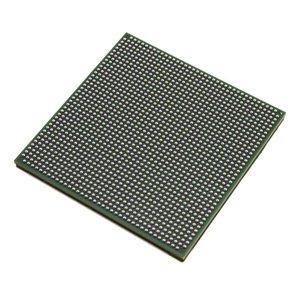
XC2V6000-6FF1517C
XC2V6000-6FF1517C ECAD Model
XC2V6000-6FF1517C Attributes
| Type | Description | Select |
|---|---|---|
| Pbfree Code | No | |
| Rohs Code | No | |
| Part Life Cycle Code | Obsolete | |
| Supply Voltage-Nom | 1.5 V | |
| Number of Inputs | 1104 | |
| Number of Outputs | 1104 | |
| Number of Logic Cells | 76032 | |
| Number of Equivalent Gates | 6000000 | |
| Number of CLBs | 8448 | |
| Combinatorial Delay of a CLB-Max | 350 ps | |
| Programmable Logic Type | FIELD PROGRAMMABLE GATE ARRAY | |
| Temperature Grade | OTHER | |
| Package Shape | SQUARE | |
| Technology | CMOS | |
| Organization | 8448 CLBS, 6000000 GATES | |
| Clock Frequency-Max | 820 MHz | |
| Power Supplies | 1.5,1.5/3.3,3.3 V | |
| Supply Voltage-Max | 1.575 V | |
| Supply Voltage-Min | 1.425 V | |
| JESD-30 Code | S-PBGA-B1517 | |
| Qualification Status | Not Qualified | |
| JESD-609 Code | e0 | |
| Moisture Sensitivity Level | 4 | |
| Operating Temperature-Max | 85 °C | |
| Peak Reflow Temperature (Cel) | 225 | |
| Time@Peak Reflow Temperature-Max (s) | 30 | |
| Number of Terminals | 1517 | |
| Package Body Material | PLASTIC/EPOXY | |
| Package Code | BGA | |
| Package Equivalence Code | BGA1517,39X39,40 | |
| Package Shape | SQUARE | |
| Package Style | GRID ARRAY | |
| Surface Mount | YES | |
| Terminal Finish | Tin/Lead (Sn63Pb37) | |
| Terminal Form | BALL | |
| Terminal Pitch | 1 mm | |
| Terminal Position | BOTTOM | |
| Width | 40 mm | |
| Length | 40 mm | |
| Seated Height-Max | 3.4 mm | |
| Ihs Manufacturer | XILINX INC | |
| Part Package Code | BGA | |
| Package Description | 40 X 40 MM, 1 MM PITCH, MS-034AAU-1, FLIP CHIP, FBGA-1517 | |
| Pin Count | 1517 | |
| Reach Compliance Code | not_compliant | |
| ECCN Code | 3A001.A.7.A | |
| HTS Code | 8542.39.00.01 |
XC2V6000-6FF1517C Datasheet Download
XC2V6000-6FF1517C Overview
The XC2V6000-6FF1517C chip model is a powerful and versatile tool for the electronics industry. It is a Field Programmable Gate Array (FPGA) chip model, which is a type of integrated circuit that is designed to be configured by a customer or a designer after manufacturing. This allows for flexibility and customization of the chip model according to the needs of the user.
The XC2V6000-6FF1517C chip model has several advantages over other FPGA chip models. It is a low-cost solution that offers a high level of performance. It has a high clock frequency of up to 600 MHz, and its reconfigurable logic blocks are also capable of performing complex operations. It also has a large number of I/O pins, which makes it suitable for a wide range of applications.
The XC2V6000-6FF1517C chip model is expected to be in high demand in the future due to its flexibility and cost-effectiveness. It can be used in a variety of applications, including automotive, industrial, and consumer electronics. It can also be used in networks and communications systems, as well as for various intelligent scenarios.
The original design intention of the XC2V6000-6FF1517C chip model was to provide a flexible and cost-effective solution for a wide range of applications. It is possible to upgrade the chip model in the future, as new technologies become available. This could enable the chip model to be used in more advanced communication systems and networks, as well as in the era of fully intelligent systems.
In summary, the XC2V6000-6FF1517C chip model is a powerful and versatile tool for the electronics industry. It is a low-cost solution that offers a high level of performance and is expected to be in high demand in the future. It can be used for a variety of applications and can be upgraded in the future to enable it to be used in more advanced communication systems and networks, as well as in the era of fully intelligent systems.
You May Also Be Interested In
3,541 In Stock
Pricing (USD)
| QTY | Unit Price | Ext Price |
|---|---|---|
| 1+ | $4,103.3088 | $4,103.3088 |
| 10+ | $4,059.1872 | $40,591.8720 |
| 100+ | $3,838.5792 | $383,857.9200 |
| 1000+ | $3,617.9712 | $1,808,985.6000 |
| 10000+ | $3,309.1200 | $3,309,120.0000 |
| The price is for reference only, please refer to the actual quotation! | ||