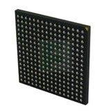
AMD Xilinx
XC2V500-4FG256C
XC2V500-4FG256C ECAD Model
XC2V500-4FG256C Attributes
| Type | Description | Select |
|---|---|---|
| Pbfree Code | No | |
| Rohs Code | No | |
| Part Life Cycle Code | Obsolete | |
| Supply Voltage-Nom | 1.5 V | |
| Number of Inputs | 172 | |
| Number of Outputs | 172 | |
| Number of Logic Cells | 6912 | |
| Number of Equivalent Gates | 500000 | |
| Number of CLBs | 768 | |
| Combinatorial Delay of a CLB-Max | 440 ps | |
| Programmable Logic Type | FIELD PROGRAMMABLE GATE ARRAY | |
| Temperature Grade | OTHER | |
| Package Shape | SQUARE | |
| Technology | CMOS | |
| Organization | 768 CLBS, 500000 GATES | |
| Clock Frequency-Max | 650 MHz | |
| Power Supplies | 1.5,1.5/3.3,3.3 V | |
| Supply Voltage-Max | 1.575 V | |
| Supply Voltage-Min | 1.425 V | |
| JESD-30 Code | S-PBGA-B256 | |
| Qualification Status | Not Qualified | |
| JESD-609 Code | e0 | |
| Moisture Sensitivity Level | 3 | |
| Operating Temperature-Max | 85 °C | |
| Peak Reflow Temperature (Cel) | 225 | |
| Time@Peak Reflow Temperature-Max (s) | 30 | |
| Number of Terminals | 256 | |
| Package Body Material | PLASTIC/EPOXY | |
| Package Code | BGA | |
| Package Equivalence Code | BGA256,16X16,40 | |
| Package Shape | SQUARE | |
| Package Style | GRID ARRAY | |
| Surface Mount | YES | |
| Terminal Finish | Tin/Lead (Sn63Pb37) | |
| Terminal Form | BALL | |
| Terminal Pitch | 1 mm | |
| Terminal Position | BOTTOM | |
| Width | 17 mm | |
| Length | 17 mm | |
| Seated Height-Max | 2 mm | |
| Ihs Manufacturer | XILINX INC | |
| Package Description | 17 X 17 MM, 1 MM PITCH, MO-034AAF-1, FBGA-256 | |
| Reach Compliance Code | not_compliant | |
| HTS Code | 8542.39.00.01 | |
| Part Package Code | BGA | |
| Pin Count | 256 | |
| ECCN Code | EAR99 |
XC2V500-4FG256C Datasheet Download
XC2V500-4FG256C Overview
Chip model XC2V500-4FG256C is a Field Programmable Gate Array (FPGA) developed by Xilinx. It is a mid-range device in the Virtex-II family with a capacity of 500K system gates. The device has four-speed grade support, ranging from -6 to -2, and 256Mb of embedded memory. It is designed to provide high-performance, low-power, and cost-effective solutions for a variety of applications.
The XC2V500-4FG256C offers a range of advantages over traditional FPGAs and other similar devices. It features a high-performance system-on-chip (SoC) architecture, which enables the integration of multiple functions on a single chip. This eliminates the need for additional components, resulting in a smaller form factor and reduced cost. Additionally, the device is designed with power efficiency in mind, allowing it to maintain a low power consumption even when running at high speeds.
The XC2V500-4FG256C is expected to be in high demand in the coming years, as it is suitable for a variety of applications. These include communications, industrial automation, medical, and consumer electronics. The device can also be used for advanced communication systems, such as 5G and Internet of Things (IoT). Furthermore, its design allows for easy upgrades and modifications, allowing users to tailor the device to their specific needs.
The XC2V500-4FG256C is designed to meet the requirements of a variety of applications. It features a high-performance system-on-chip architecture, 256Mb of embedded memory, and four-speed grades ranging from -6 to -2. It also supports a wide range of protocols and interfaces, including Ethernet, USB, and PCI Express. Additionally, the device is designed with power efficiency in mind, allowing it to maintain a low power consumption even when running at high speeds.
In order to ensure that the XC2V500-4FG256C meets the needs of its users, it is important to consider the specific design requirements of the device. This includes the power requirements, the operating temperature range, and the clock speed. Additionally, the device should be tested to ensure that it meets the required performance levels. Furthermore, it is important to consider any potential issues that may arise during the design process, such as potential compatibility issues or power supply problems.
The XC2V500-4FG256C has been successfully applied in a number of case studies. In one example, the device was used to develop a high-speed, low-power, and cost-effective solution for a communication system. In another example, the device was used to develop a low-power and low-cost industrial automation system. These studies demonstrate the versatility and reliability of the XC2V500-4FG256C.
In conclusion, the XC2V500-4FG256C is a high-performance, low-power, and cost-effective FPGA device. It is expected to be in high demand in the coming years, as it is suitable for a variety of applications. Additionally, its design allows for easy upgrades and modifications, allowing users to tailor the device to their specific needs. Furthermore, it is important to consider the specific design requirements of the device, as well as any potential issues that may arise during the design process.
You May Also Be Interested In
4,342 In Stock
Pricing (USD)
| QTY | Unit Price | Ext Price |
|---|---|---|
| 1+ | $69.5640 | $69.5640 |
| 10+ | $68.8160 | $688.1600 |
| 100+ | $65.0760 | $6,507.6000 |
| 1000+ | $61.3360 | $30,668.0000 |
| 10000+ | $56.1000 | $56,100.0000 |
| The price is for reference only, please refer to the actual quotation! | ||
