AMD Xilinx
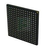
XC2V40-6FG256C
XC2V40-6FG256C ECAD Model
XC2V40-6FG256C Attributes
| Type | Description | Select |
|---|---|---|
| Pbfree Code | No | |
| Rohs Code | No | |
| Part Life Cycle Code | Obsolete | |
| Supply Voltage-Nom | 1.5 V | |
| Number of Inputs | 88 | |
| Number of Outputs | 88 | |
| Number of Logic Cells | 576 | |
| Number of Equivalent Gates | 40000 | |
| Number of CLBs | 64 | |
| Combinatorial Delay of a CLB-Max | 350 ps | |
| Programmable Logic Type | FIELD PROGRAMMABLE GATE ARRAY | |
| Temperature Grade | OTHER | |
| Package Shape | SQUARE | |
| Technology | CMOS | |
| Organization | 64 CLBS, 40000 GATES | |
| Clock Frequency-Max | 820 MHz | |
| Power Supplies | 1.5,1.5/3.3,3.3 V | |
| Supply Voltage-Max | 1.575 V | |
| Supply Voltage-Min | 1.425 V | |
| JESD-30 Code | S-PBGA-B256 | |
| Qualification Status | Not Qualified | |
| JESD-609 Code | e0 | |
| Moisture Sensitivity Level | 3 | |
| Operating Temperature-Max | 85 °C | |
| Peak Reflow Temperature (Cel) | 225 | |
| Time@Peak Reflow Temperature-Max (s) | 30 | |
| Number of Terminals | 256 | |
| Package Body Material | PLASTIC/EPOXY | |
| Package Code | BGA | |
| Package Equivalence Code | BGA256,16X16,40 | |
| Package Shape | SQUARE | |
| Package Style | GRID ARRAY | |
| Surface Mount | YES | |
| Terminal Finish | Tin/Lead (Sn63Pb37) | |
| Terminal Form | BALL | |
| Terminal Pitch | 1 mm | |
| Terminal Position | BOTTOM | |
| Width | 17 mm | |
| Length | 17 mm | |
| Seated Height-Max | 2 mm | |
| Ihs Manufacturer | XILINX INC | |
| Part Package Code | BGA | |
| Package Description | 17 X 17 MM, 1 MM PITCH, MO-034AAF-1, FBGA-256 | |
| Pin Count | 256 | |
| Reach Compliance Code | not_compliant | |
| HTS Code | 8542.39.00.01 | |
| ECCN Code | EAR99 |
XC2V40-6FG256C Datasheet Download
XC2V40-6FG256C Overview
The chip model XC2V40-6FG256C is a field programmable gate array (FPGA) designed for high-performance digital signal processing, embedded processing, and image processing. It is an ideal choice for those who need to use HDL language to achieve their desired goals.
The original design intention of the chip model XC2V40-6FG256C was to provide users with a powerful and versatile platform for their digital signal processing, embedded processing, and image processing applications. The XC2V40-6FG256C has the capability to be upgraded in the future, allowing users to increase its performance and capabilities. This makes it a great choice for advanced communication systems, as it can be updated and improved as technology advances.
The XC2V40-6FG256C can also be applied to the development and popularization of future intelligent robots. Its high-performance capabilities, combined with its ability to be upgraded, make it a great choice for those looking to create intelligent robots. To make the most of the XC2V40-6FG256C, technical talents are needed to use the model effectively. Knowledge of HDL language and digital signal processing, embedded processing, and image processing are essential for those looking to make the most of the XC2V40-6FG256C. With the right knowledge and expertise, the XC2V40-6FG256C can be used to create powerful and capable robots.
In conclusion, the XC2V40-6FG256C is an excellent choice for those looking to utilize HDL language for their digital signal processing, embedded processing, and image processing applications. Its ability to be upgraded makes it a great choice for advanced communication systems, as well as for the development and popularization of future intelligent robots. To make the most of the XC2V40-6FG256C, technical talents are needed to use the model effectively. With the right knowledge and expertise, the XC2V40-6FG256C can be used to create powerful and capable robots.
You May Also Be Interested In
2,491 In Stock
Pricing (USD)
| QTY | Unit Price | Ext Price |
|---|---|---|
| No reference price found. | ||
