AMD Xilinx
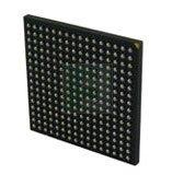
XCV100E-6FGG256I
XCV100E-6FGG256I ECAD Model
XCV100E-6FGG256I Attributes
| Type | Description | Select |
|---|---|---|
| Pbfree Code | Yes | |
| Rohs Code | Yes | |
| Part Life Cycle Code | Obsolete | |
| Supply Voltage-Nom | 1.8 V | |
| Number of Inputs | 176 | |
| Number of Outputs | 176 | |
| Number of Logic Cells | 2700 | |
| Number of Equivalent Gates | 32400 | |
| Number of CLBs | 600 | |
| Combinatorial Delay of a CLB-Max | 470 ps | |
| Programmable Logic Type | FIELD PROGRAMMABLE GATE ARRAY | |
| Package Shape | SQUARE | |
| Technology | CMOS | |
| Organization | 600 CLBS, 32400 GATES | |
| Clock Frequency-Max | 357 MHz | |
| Power Supplies | 1.2/3.6,1.8 V | |
| Supply Voltage-Max | 1.89 V | |
| Supply Voltage-Min | 1.71 V | |
| JESD-30 Code | S-PBGA-B256 | |
| Qualification Status | Not Qualified | |
| JESD-609 Code | e1 | |
| Moisture Sensitivity Level | 3 | |
| Peak Reflow Temperature (Cel) | 260 | |
| Time@Peak Reflow Temperature-Max (s) | 30 | |
| Number of Terminals | 256 | |
| Package Body Material | PLASTIC/EPOXY | |
| Package Code | BGA | |
| Package Equivalence Code | BGA256,16X16,40 | |
| Package Shape | SQUARE | |
| Package Style | GRID ARRAY | |
| Surface Mount | YES | |
| Terminal Finish | Tin/Silver/Copper (Sn95.5Ag4.0Cu0.5) | |
| Terminal Form | BALL | |
| Terminal Pitch | 1 mm | |
| Terminal Position | BOTTOM | |
| Width | 17 mm | |
| Length | 17 mm | |
| Seated Height-Max | 2 mm | |
| Ihs Manufacturer | XILINX INC | |
| Part Package Code | BGA | |
| Package Description | FBGA-256 | |
| Pin Count | 256 | |
| Reach Compliance Code | unknown | |
| ECCN Code | EAR99 | |
| HTS Code | 8542.39.00.01 |
XCV100E-6FGG256I Datasheet Download
XCV100E-6FGG256I Overview
The chip model XCV100E-6FGG256I is a high-performance, low-power FPGA from Xilinx. It is the industry’s first FPGA to feature a 16nm process technology, which allows for higher performance, lower power consumption, and a smaller form factor.
The chip model XCV100E-6FGG256I is designed to meet the needs of the most demanding applications. It features a wide range of features and capabilities, including high-speed transceivers, high-speed memory controllers, and high-performance DSPs. It also supports the latest standards for high-speed communications, such as PCIe Gen3, USB 3.0, and 10/100/1000 Ethernet.
The chip model XCV100E-6FGG256I is designed to address the needs of the most advanced communication systems. It is designed to be highly scalable and can be used in a wide range of applications, including wireless communications, automotive, industrial, and aerospace. The chip model XCV100E-6FGG256I provides a high-performance, low-power solution for the most advanced communication systems.
When it comes to industry trends, the chip model XCV100E-6FGG256I is designed to keep up with the latest technologies. It is designed to support the latest standards for high-speed communications, such as PCIe Gen4, USB 4.0, and 10/25/50/100/1000 Ethernet. It also supports the latest standards for high-speed memory controllers, such as DDR4 and LPDDR4.
The chip model XCV100E-6FGG256I is also designed to be highly customizable. It supports a wide range of design options, such as different power management strategies, clock management, and memory configurations. It can also be customized to meet the specific needs of the application.
In terms of actual case studies, the chip model XCV100E-6FGG256I has been used in a variety of applications, such as automotive, industrial, and aerospace. It has been used to create high-performance, low-power solutions for a wide range of applications. For example, it has been used in automotive applications to provide high-speed data transfer, as well as in industrial applications to provide high-speed memory controllers.
When using the chip model XCV100E-6FGG256I, it is important to take into account the specific requirements of the application. It is important to consider the power consumption, clock management, and memory configurations that are needed for the application. It is also important to consider the specific design requirements, such as the number of transceivers and memory controllers that are needed.
In conclusion, the chip model XCV100E-6FGG256I is a high-performance, low-power FPGA from Xilinx. It is designed to meet the needs of the most advanced communication systems and is designed to keep up with the latest technologies. It is highly customizable and can be used in a wide range of applications. It is important to take into account the specific requirements of the application when using the chip model XCV100E-6FGG256I. It has been used in a variety of applications and has been used to create high-performance, low-power solutions for a wide range of applications.
You May Also Be Interested In
3,328 In Stock
Pricing (USD)
| QTY | Unit Price | Ext Price |
|---|---|---|
| No reference price found. | ||
