
AMD Xilinx
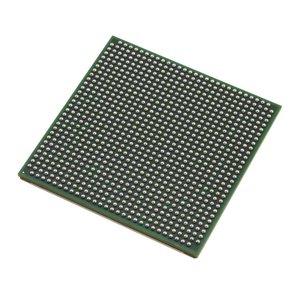
XC2VPX20-6FFG896C
XC2VPX20-6FFG896C ECAD Model
XC2VPX20-6FFG896C Attributes
| Type | Description | Select |
|---|---|---|
| Rohs Code | Yes | |
| Part Life Cycle Code | Obsolete | |
| Supply Voltage-Nom | 1.5 V | |
| Number of Inputs | 552 | |
| Number of Outputs | 552 | |
| Number of Logic Cells | 22032 | |
| Number of CLBs | 2448 | |
| Combinatorial Delay of a CLB-Max | 320 ps | |
| Programmable Logic Type | FIELD PROGRAMMABLE GATE ARRAY | |
| Temperature Grade | OTHER | |
| Package Shape | SQUARE | |
| Technology | CMOS | |
| Organization | 2448 CLBS | |
| Clock Frequency-Max | 1.2 GHz | |
| Power Supplies | 1.5,1.5/3.3,2/2.5,2.5 V | |
| Supply Voltage-Max | 1.575 V | |
| Supply Voltage-Min | 1.425 V | |
| JESD-30 Code | S-PBGA-B896 | |
| Qualification Status | Not Qualified | |
| JESD-609 Code | e1 | |
| Moisture Sensitivity Level | 4 | |
| Operating Temperature-Max | 85 °C | |
| Peak Reflow Temperature (Cel) | 245 | |
| Time@Peak Reflow Temperature-Max (s) | 30 | |
| Number of Terminals | 896 | |
| Package Body Material | PLASTIC/EPOXY | |
| Package Code | BGA | |
| Package Equivalence Code | BGA896,30X30,40 | |
| Package Shape | SQUARE | |
| Package Style | GRID ARRAY | |
| Surface Mount | YES | |
| Terminal Finish | Tin/Silver/Copper (Sn95.5Ag4.0Cu0.5) | |
| Terminal Form | BALL | |
| Terminal Pitch | 1 mm | |
| Terminal Position | BOTTOM | |
| Width | 31 mm | |
| Length | 31 mm | |
| Seated Height-Max | 3.4 mm | |
| Ihs Manufacturer | XILINX INC | |
| Part Package Code | BGA | |
| Package Description | 31 X 31 MM, 1 MM PITCH, MS-034AAN-1, FCBGA-896 | |
| Pin Count | 896 | |
| Reach Compliance Code | not_compliant | |
| HTS Code | 8542.39.00.01 |
XC2VPX20-6FFG896C Datasheet Download
XC2VPX20-6FFG896C Overview
The XC2VPX20-6FFG896C chip model is a high-performance, low-power FPGA that offers a wide range of features and capabilities. It is designed to meet the needs of a variety of applications, ranging from digital signal processing to embedded systems. This chip model is a perfect fit for applications that require a high degree of flexibility and scalability.
The XC2VPX20-6FFG896C chip model is designed to provide a high degree of performance and flexibility. It is equipped with a variety of features, such as an on-board memory controller, a high-speed transceiver, and an advanced power management system. These features make the chip model suitable for a wide range of applications, including digital signal processing, embedded systems, and communication systems.
The XC2VPX20-6FFG896C chip model offers a wide range of advantages, such as low power consumption, high performance, and scalability. It is also designed with a high degree of flexibility, allowing for the design of custom solutions. Additionally, the chip model is compatible with a variety of industry-standard interfaces and protocols, making it an ideal choice for a variety of applications.
The XC2VPX20-6FFG896C chip model is expected to be in high demand in the coming years, as it is well-suited for a variety of applications. It is expected to be used in a variety of industries, including automotive, industrial, and medical. Additionally, the chip model is expected to be used in advanced communication systems, as it is designed with a high degree of flexibility and scalability.
The product description and design requirements of the XC2VPX20-6FFG896C chip model are as follows. The chip model is a high-performance, low-power FPGA that offers a wide range of features and capabilities. It is designed with a variety of features, such as an on-board memory controller, a high-speed transceiver, and an advanced power management system. Additionally, the chip model is compatible with a variety of industry-standard interfaces and protocols, making it an ideal choice for a variety of applications.
When designing with the XC2VPX20-6FFG896C chip model, there are several things to consider. First, the chip model should be designed with the specific requirements of the application in mind. Additionally, the chip model should be tested thoroughly prior to deployment to ensure that it meets the requirements of the application. Finally, the chip model should be designed with an eye towards future upgrades, as it is designed with a high degree of flexibility and scalability.
In conclusion, the XC2VPX20-6FFG896C chip model is a high-performance, low-power FPGA that offers a wide range of features and capabilities. It is designed to meet the needs of a variety of applications, ranging from digital signal processing to embedded systems. The chip model offers a wide range of advantages, such as low power consumption, high performance, and scalability. Additionally, the chip model is expected to be in high demand in the coming years, as it is well-suited for a variety of applications. Finally, when designing with the XC2VPX20-6FFG896C chip model, it should be designed with the specific requirements of the application in mind, tested thoroughly prior to deployment, and designed with an eye towards future upgrades.
You May Also Be Interested In
3,643 In Stock
Pricing (USD)
| QTY | Unit Price | Ext Price |
|---|---|---|
| No reference price found. | ||