
AMD Xilinx
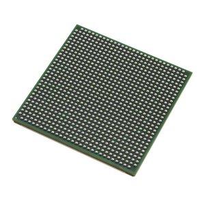
XC2VPX20-5FFG896C
XC2VPX20-5FFG896C ECAD Model
XC2VPX20-5FFG896C Attributes
| Type | Description | Select |
|---|---|---|
| Rohs Code | Yes | |
| Part Life Cycle Code | Obsolete | |
| Supply Voltage-Nom | 1.5 V | |
| Number of Inputs | 552 | |
| Number of Outputs | 552 | |
| Number of Logic Cells | 22032 | |
| Number of CLBs | 2448 | |
| Combinatorial Delay of a CLB-Max | 360 ps | |
| Programmable Logic Type | FIELD PROGRAMMABLE GATE ARRAY | |
| Temperature Grade | OTHER | |
| Package Shape | SQUARE | |
| Technology | CMOS | |
| Organization | 2448 CLBS | |
| Clock Frequency-Max | 1.05 GHz | |
| Power Supplies | 1.5,1.5/3.3,2/2.5,2.5 V | |
| Supply Voltage-Max | 1.575 V | |
| Supply Voltage-Min | 1.425 V | |
| JESD-30 Code | S-PBGA-B896 | |
| Qualification Status | Not Qualified | |
| JESD-609 Code | e1 | |
| Moisture Sensitivity Level | 4 | |
| Operating Temperature-Max | 85 °C | |
| Peak Reflow Temperature (Cel) | 245 | |
| Time@Peak Reflow Temperature-Max (s) | 30 | |
| Number of Terminals | 896 | |
| Package Body Material | PLASTIC/EPOXY | |
| Package Code | BGA | |
| Package Equivalence Code | BGA896,30X30,40 | |
| Package Shape | SQUARE | |
| Package Style | GRID ARRAY | |
| Surface Mount | YES | |
| Terminal Finish | Tin/Silver/Copper (Sn95.5Ag4.0Cu0.5) | |
| Terminal Form | BALL | |
| Terminal Pitch | 1 mm | |
| Terminal Position | BOTTOM | |
| Width | 31 mm | |
| Length | 31 mm | |
| Seated Height-Max | 3.4 mm | |
| Ihs Manufacturer | XILINX INC | |
| Part Package Code | BGA | |
| Package Description | 31 X 31 MM, 1 MM PITCH, MS-034AAN-1, FCBGA-896 | |
| Pin Count | 896 | |
| Reach Compliance Code | not_compliant | |
| HTS Code | 8542.39.00.01 |
XC2VPX20-5FFG896C Datasheet Download
XC2VPX20-5FFG896C Overview
The XC2VPX20-5FFG896C chip model is a high-performance, versatile processor designed for a variety of applications. It is suitable for digital signal processing, embedded processing, image processing, and other tasks that require the use of HDL language. This chip model has a number of advantages that make it attractive to many industries.
First, the XC2VPX20-5FFG896C chip model is powerful enough to handle a variety of tasks. It has a large number of transistors and a wide range of instructions, allowing it to process data quickly and accurately. Additionally, it is capable of handling a variety of tasks in parallel, making it an ideal choice for applications that require a high degree of multitasking.
Second, the XC2VPX20-5FFG896C chip model is highly efficient. It consumes less power than other chips, making it an attractive option for companies looking to reduce their energy costs. Additionally, it is designed to be upgradeable, allowing companies to easily upgrade their hardware without needing to purchase new hardware.
Third, the XC2VPX20-5FFG896C chip model is cost-effective. It is relatively inexpensive compared to other chips, making it an attractive option for companies looking to save money. Additionally, it is designed to be reliable, allowing companies to trust that their data is safe and secure.
Given the advantages of the XC2VPX20-5FFG896C chip model, it is expected that demand for this chip model will continue to grow in the future. In particular, it is likely to be used in a variety of network applications, including wireless networks, cellular networks, and the Internet of Things. Additionally, it is expected to be used in a variety of intelligent scenarios, such as self-driving cars and smart homes. Finally, it is likely that the XC2VPX20-5FFG896C chip model will be used in the era of fully intelligent systems, allowing for the development of more sophisticated and efficient systems.
You May Also Be Interested In
2,821 In Stock
Pricing (USD)
| QTY | Unit Price | Ext Price |
|---|---|---|
| No reference price found. | ||