

AMD Xilinx
XCZU48DR-L2FSVE1156I
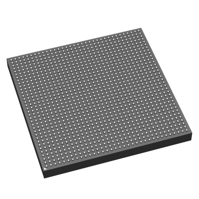
XCZU48DR-L2FSVE1156I ECAD Model
XCZU48DR-L2FSVE1156I Attributes
| Type | Description | Select |
|---|---|---|
| Rohs Code | Yes | |
| Part Life Cycle Code | Active | |
| Surface Mount | YES | |
| Supply Voltage-Nom | 720 mV | |
| uPs/uCs/Peripheral ICs Type | PROGRAMMABLE SoC | |
| Technology | CMOS | |
| Supply Voltage-Max | 742 mV | |
| Supply Voltage-Min | 698 mV | |
| Temperature Grade | INDUSTRIAL | |
| JESD-30 Code | R-PBGA-B1156 | |
| JESD-609 Code | e1 | |
| Moisture Sensitivity Level | 4 | |
| Operating Temperature-Max | 100 °C | |
| Operating Temperature-Min | -40 °C | |
| Peak Reflow Temperature (Cel) | 240 | |
| Time@Peak Reflow Temperature-Max (s) | 30 | |
| Number of Terminals | 1156 | |
| Package Body Material | PLASTIC/EPOXY | |
| Package Code | BGA | |
| Package Shape | RECTANGULAR | |
| Package Style | GRID ARRAY | |
| Terminal Finish | TIN SILVER COPPER | |
| Terminal Form | BALL | |
| Terminal Position | BOTTOM | |
| Ihs Manufacturer | XILINX INC | |
| Reach Compliance Code | compliant | |
| ECCN Code | 5A002.A.4 | |
| HTS Code | 8542.39.00.01 | |
| Package Description | FLIPCHIP-1156 | |
| Date Of Intro | 2019-02-20 |
XCZU48DR-L2FSVE1156I Datasheet Download
XCZU48DR-L2FSVE1156I Overview
The XCZU48DR-L2FSVE1156I chip model is a powerful and versatile integrated circuit designed for high-performance digital signal processing, embedded processing, image processing, and other applications. It is based on the Xilinx UltraScale+ architecture and is ideal for applications requiring the use of HDL language. The chip model is designed to meet the needs of advanced communication systems and can be easily upgraded to meet future requirements.
The XCZU48DR-L2FSVE1156I chip model is built with a wide range of features, such as a dual-core ARM Cortex-A53 processor, high-speed memory, and a high-performance FPGA. It also includes a wide range of peripherals, including PCIe, USB, and Ethernet. The chip model is designed to be highly scalable and can be used in a wide variety of applications.
In terms of product description, the XCZU48DR-L2FSVE1156I chip model is designed to be easily integrated into existing systems. It is designed for use in high-performance applications and requires the use of HDL language. The chip model is also designed to be highly reliable and has built-in safety features to protect against power surges and other environmental factors.
When it comes to specific design requirements, the XCZU48DR-L2FSVE1156I chip model requires the use of Xilinx Vivado Design Suite for development and debugging. Additionally, the chip model requires the use of the Xilinx UltraScale+ architecture, which is specifically designed to meet the needs of advanced communication systems.
In terms of case studies, the XCZU48DR-L2FSVE1156I chip model has been used in a variety of applications, such as embedded systems, medical imaging, and industrial automation. In each of these applications, the chip model has demonstrated its ability to meet the needs of the specific application. Additionally, the chip model has been used in a variety of research projects, such as image processing and machine learning.
Finally, when using the XCZU48DR-L2FSVE1156I chip model, it is important to take the necessary precautions. It is important to ensure that the chip model is properly installed and configured, and that the correct HDL language is used. Additionally, it is important to ensure that the chip model is properly powered and cooled. By following these precautions, users can ensure that the chip model performs as expected.
You May Also Be Interested In
3,749 In Stock
Pricing (USD)
| QTY | Unit Price | Ext Price |
|---|---|---|
| No reference price found. | ||