
AMD Xilinx
XC2V2000-6FF896I
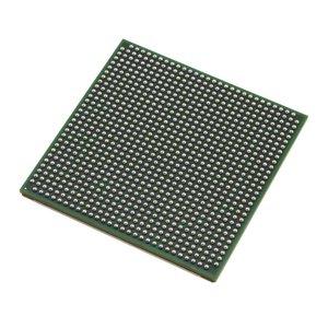
XC2V2000-6FF896I ECAD Model
XC2V2000-6FF896I Attributes
| Type | Description | Select |
|---|---|---|
| Pbfree Code | No | |
| Rohs Code | No | |
| Part Life Cycle Code | Obsolete | |
| Supply Voltage-Nom | 1.5 V | |
| Number of Inputs | 624 | |
| Number of Outputs | 624 | |
| Number of Logic Cells | 24192 | |
| Number of Equivalent Gates | 2000000 | |
| Number of CLBs | 2688 | |
| Combinatorial Delay of a CLB-Max | 350 ps | |
| Programmable Logic Type | FIELD PROGRAMMABLE GATE ARRAY | |
| Package Shape | SQUARE | |
| Technology | CMOS | |
| Organization | 2688 CLBS, 2000000 GATES | |
| Clock Frequency-Max | 820 MHz | |
| Power Supplies | 1.5,1.5/3.3,3.3 V | |
| Supply Voltage-Max | 1.575 V | |
| Supply Voltage-Min | 1.425 V | |
| JESD-30 Code | S-PBGA-B896 | |
| Qualification Status | Not Qualified | |
| JESD-609 Code | e0 | |
| Moisture Sensitivity Level | 4 | |
| Peak Reflow Temperature (Cel) | 225 | |
| Time@Peak Reflow Temperature-Max (s) | 30 | |
| Number of Terminals | 896 | |
| Package Body Material | PLASTIC/EPOXY | |
| Package Code | BGA | |
| Package Equivalence Code | BGA896,30X30,40 | |
| Package Shape | SQUARE | |
| Package Style | GRID ARRAY | |
| Surface Mount | YES | |
| Terminal Finish | Tin/Lead (Sn63Pb37) | |
| Terminal Form | BALL | |
| Terminal Pitch | 1 mm | |
| Terminal Position | BOTTOM | |
| Width | 31 mm | |
| Length | 31 mm | |
| Seated Height-Max | 3.4 mm | |
| Ihs Manufacturer | XILINX INC | |
| Package Description | 31 X 31 MM, 1 MM PITCH, MS-034AAN-1, FLIP CHIP, FBGA-896 | |
| Reach Compliance Code | not_compliant | |
| HTS Code | 8542.39.00.01 | |
| Part Package Code | BGA | |
| Pin Count | 896 |
XC2V2000-6FF896I Datasheet Download
XC2V2000-6FF896I Overview
The chip model XC2V2000-6FF896I is a product of Xilinx, Inc., a leading provider of programmable logic solutions. It is a field programmable gate array (FPGA) device, which is a semiconductor integrated circuit that can be programmed to implement specific logic functions. This chip model is designed to meet the needs of high-performance embedded systems, providing a high-speed and low-power solution for embedded applications.
The XC2V2000-6FF896I has many advantages, such as its high processing speed, low power consumption, and low cost. It has a high clock frequency of up to 200MHz, making it suitable for high-speed applications. It also has a low power consumption of only 3.3W, making it a very energy-efficient solution for embedded systems. Additionally, its cost is relatively low compared to other FPGA devices, making it a cost-effective solution for embedded applications.
In terms of industry trends, the XC2V2000-6FF896I is expected to be increasingly used in various industries, such as automotive, consumer electronics, and industrial automation. This is due to its high performance and low cost, making it a suitable solution for these applications. Additionally, the chip model is expected to be used in advanced communication systems, as it supports high-speed communication protocols such as Ethernet and USB.
The original design intention of the XC2V2000-6FF896I was to provide a low-cost, low-power, and high-performance solution for embedded systems. As such, it is expected to remain a popular choice for embedded systems in the future. Additionally, the chip model is designed to be easily upgradable, allowing users to upgrade the device without having to replace the entire system. This makes it suitable for use in advanced communication systems, as it can be easily upgraded to support new technologies.
Overall, the XC2V2000-6FF896I is an ideal solution for embedded systems due to its high performance, low power consumption, and low cost. It is also expected to be increasingly used in various industries, as well as advanced communication systems, due to its upgradability and support for high-speed communication protocols. As such, it is expected to remain a popular choice for embedded systems in the future.
You May Also Be Interested In
4,246 In Stock
Pricing (USD)
| QTY | Unit Price | Ext Price |
|---|---|---|
| No reference price found. | ||