
AMD Xilinx
XC2V1000-6FF896I
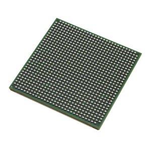
XC2V1000-6FF896I ECAD Model
XC2V1000-6FF896I Attributes
| Type | Description | Select |
|---|---|---|
| Pbfree Code | No | |
| Rohs Code | No | |
| Part Life Cycle Code | Obsolete | |
| Supply Voltage-Nom | 1.5 V | |
| Number of Inputs | 432 | |
| Number of Outputs | 432 | |
| Number of Logic Cells | 11520 | |
| Number of Equivalent Gates | 1000000 | |
| Number of CLBs | 1280 | |
| Combinatorial Delay of a CLB-Max | 350 ps | |
| Programmable Logic Type | FIELD PROGRAMMABLE GATE ARRAY | |
| Package Shape | SQUARE | |
| Technology | CMOS | |
| Organization | 1280 CLBS, 1000000 GATES | |
| Clock Frequency-Max | 820 MHz | |
| Power Supplies | 1.5,1.5/3.3,3.3 V | |
| Supply Voltage-Max | 1.575 V | |
| Supply Voltage-Min | 1.425 V | |
| JESD-30 Code | S-PBGA-B896 | |
| Qualification Status | Not Qualified | |
| JESD-609 Code | e0 | |
| Moisture Sensitivity Level | 4 | |
| Peak Reflow Temperature (Cel) | 225 | |
| Time@Peak Reflow Temperature-Max (s) | 30 | |
| Number of Terminals | 896 | |
| Package Body Material | PLASTIC/EPOXY | |
| Package Code | BGA | |
| Package Equivalence Code | BGA896,30X30,40 | |
| Package Shape | SQUARE | |
| Package Style | GRID ARRAY | |
| Surface Mount | YES | |
| Terminal Finish | Tin/Lead (Sn63Pb37) | |
| Terminal Form | BALL | |
| Terminal Pitch | 1 mm | |
| Terminal Position | BOTTOM | |
| Width | 31 mm | |
| Length | 31 mm | |
| Seated Height-Max | 3.4 mm | |
| Ihs Manufacturer | XILINX INC | |
| Part Package Code | BGA | |
| Package Description | 31 X 31 MM, 1 MM PITCH, MS-034AAN-1, FLIP CHIP, FBGA-896 | |
| Pin Count | 896 | |
| Reach Compliance Code | not_compliant | |
| HTS Code | 8542.39.00.01 |
XC2V1000-6FF896I Datasheet Download
XC2V1000-6FF896I Overview
The chip model XC2V1000-6FF896I is the latest generation of Xilinx FPGA technology, designed for high-performance applications requiring high reliability and low power consumption. This model is designed to support a wide range of applications, including communications, networking, and embedded systems. It is also suitable for a variety of industrial and automotive applications.
The XC2V1000-6FF896I is designed to provide high performance, reliability, and low power consumption. It supports multiple clock domains, multiple I/O banks, and a variety of memory interfaces. It also includes a range of advanced features, such as high-speed transceivers, configurable logic blocks, and multiple clock sources. Additionally, the chip model is designed for easy integration into existing systems, as well as for future upgrades.
The XC2V1000-6FF896I is well-suited for a variety of applications, including advanced communication systems, networks, and embedded systems. It can be used in a variety of intelligent scenarios, such as the Internet of Things (IoT), artificial intelligence (AI), and machine learning (ML). It is also suitable for use in the era of fully intelligent systems, as it can be used to develop intelligent solutions for a variety of applications.
The XC2V1000-6FF896I is designed to meet the industry's ever-changing needs. Its advanced features and low power consumption make it an ideal choice for a variety of applications. As the industry continues to evolve, the chip model can be upgraded to meet the needs of the future. In addition, it can be used in a variety of intelligent scenarios, such as the Internet of Things, artificial intelligence, and machine learning. The chip model can also be used in the era of fully intelligent systems, as it can be used to develop intelligent solutions for a variety of applications.
You May Also Be Interested In
1,729 In Stock
Pricing (USD)
| QTY | Unit Price | Ext Price |
|---|---|---|
| No reference price found. | ||