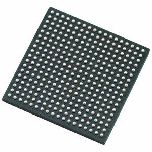
AMD Xilinx
XC2C384-10FG324C
XC2C384-10FG324C ECAD Model
XC2C384-10FG324C Attributes
| Type | Description | Select |
|---|---|---|
| Pbfree Code | No | |
| Rohs Code | No | |
| Part Life Cycle Code | Active | |
| Supply Voltage-Nom | 1.8 V | |
| Propagation Delay | 10 ns | |
| Number of Inputs | 240 | |
| Number of Outputs | 240 | |
| Number of Macro Cells | 384 | |
| Number of I/O Lines | 240 | |
| Programmable Logic Type | FLASH PLD | |
| Temperature Grade | COMMERCIAL | |
| Package Shape | SQUARE | |
| Technology | CMOS | |
| Organization | 0 DEDICATED INPUTS, 240 I/O | |
| Additional Feature | YES | |
| Architecture | PLA-TYPE | |
| Clock Frequency-Max | 83 MHz | |
| In-System Programmable | YES | |
| JTAG BST | YES | |
| Output Function | MACROCELL | |
| Power Supplies | 1.5/3.3,1.8 V | |
| Supply Voltage-Max | 1.9 V | |
| Supply Voltage-Min | 1.7 V | |
| JESD-30 Code | S-PBGA-B324 | |
| Qualification Status | Not Qualified | |
| JESD-609 Code | e0 | |
| Moisture Sensitivity Level | 3 | |
| Operating Temperature-Max | 70 °C | |
| Peak Reflow Temperature (Cel) | 225 | |
| Time@Peak Reflow Temperature-Max (s) | 30 | |
| Number of Terminals | 324 | |
| Package Body Material | PLASTIC/EPOXY | |
| Package Code | BGA | |
| Package Equivalence Code | BGA324,22X22,40 | |
| Package Shape | SQUARE | |
| Package Style | GRID ARRAY | |
| Surface Mount | YES | |
| Terminal Finish | TIN LEAD | |
| Terminal Form | BALL | |
| Terminal Pitch | 1 mm | |
| Terminal Position | BOTTOM | |
| Width | 23 mm | |
| Length | 23 mm | |
| Seated Height-Max | 2.5 mm | |
| Ihs Manufacturer | XILINX INC | |
| Part Package Code | BGA | |
| Package Description | 23 X 23 MM, 1 MM PITCH, FBGA-324 | |
| Pin Count | 324 | |
| Reach Compliance Code | not_compliant | |
| ECCN Code | 3A991.D | |
| HTS Code | 8542.39.00.01 |
XC2C384-10FG324C Datasheet Download
XC2C384-10FG324C Overview
The chip model XC2C384-10FG324C is a highly advanced semiconductor device designed for use in a wide variety of applications. This model is manufactured by Xilinx, a leading provider of programmable logic components. It is a low-power, high-performance, low-cost FPGA with a wide range of features and capabilities.
The XC2C384-10FG324C is designed to offer significant advantages over other FPGAs. It is capable of providing faster processing speeds than traditional FPGAs, while also consuming less energy. This makes it an attractive choice for applications that require high performance and low power consumption. Additionally, the XC2C384-10FG324C is highly configurable, allowing users to customize their designs to meet specific requirements.
When it comes to industry trends, the XC2C384-10FG324C is well-suited for use in a variety of applications. It is an ideal choice for embedded systems, communications systems, and other industrial applications. As technology advances, the XC2C384-10FG324C is likely to remain a popular choice for many applications.
Regarding the future development of related industries, the XC2C384-10FG324C is likely to remain an important component of many applications. It is likely that new technologies will be needed to support the application environment, but the exact requirements will depend on the specific application.
The original design intention of the XC2C384-10FG324C was to provide a low-cost, high-performance FPGA with a wide range of features and capabilities. It was designed to be highly configurable and capable of providing faster processing speeds than traditional FPGAs while consuming less energy.
It is possible to upgrade the XC2C384-10FG324C, but it is important to consider the specific requirements of the application before making any changes. Additionally, it is important to understand the potential risks associated with making such an upgrade.
When it comes to product description and design requirements, the XC2C384-10FG324C is a highly advanced semiconductor device designed for use in a wide variety of applications. It is a low-power, high-performance, low-cost FPGA with a wide range of features and capabilities. The device is highly configurable and capable of providing faster processing speeds than traditional FPGAs while consuming less energy.
In order to ensure the success of any project involving the XC2C384-10FG324C, it is important to understand the specific requirements of the application and the potential risks associated with making any changes. Additionally, it is important to consider actual case studies and any potential precautions that may be necessary.
In conclusion, the XC2C384-10FG324C is a highly advanced semiconductor device designed for use in a wide variety of applications. It is capable of providing faster processing speeds than traditional FPGAs while also consuming less energy. It is likely to remain an important component of many applications, and new technologies may be needed to support the application environment. Additionally, it is important to understand the original design intention of the XC2C384-10FG324C, the possibility of future upgrades, and the product description and design requirements. Understanding these aspects is essential for ensuring the success of any project involving the XC2C384-10FG324C.
You May Also Be Interested In
1,741 In Stock
Pricing (USD)
| QTY | Unit Price | Ext Price |
|---|---|---|
| 1+ | $107.5043 | $107.5043 |
| 10+ | $106.3483 | $1,063.4832 |
| 100+ | $100.5685 | $10,056.8520 |
| 1000+ | $94.7887 | $47,394.3600 |
| 10000+ | $86.6970 | $86,697.0000 |
| The price is for reference only, please refer to the actual quotation! | ||
