
Intel Corporation
EP1K50TC144-2N
EP1K50TC144-2N ECAD Model
EP1K50TC144-2N Attributes
| Type | Description | Select |
|---|---|---|
| Mfr | Intel | |
| Series | ACEX-1K® | |
| Package | Tray | |
| Number of LABs/CLBs | 360 | |
| Number of Logic Elements/Cells | 2880 | |
| Total RAM Bits | 40960 | |
| Number of I/O | 102 | |
| Number of Gates | 199000 | |
| Voltage - Supply | 2.375V ~ 2.625V | |
| Mounting Type | Surface Mount | |
| Operating Temperature | 0°C ~ 70°C (TA) | |
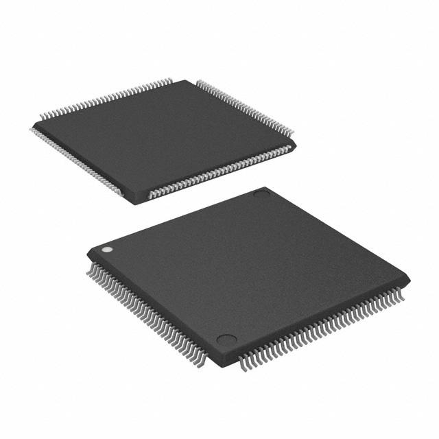
| Package / Case | 144-LQFP | |
| Supplier Device Package | 144-TQFP (20x20) | |
| Base Product Number | EP1K50 |
EP1K50TC144-2N Datasheet Download
EP1K50TC144-2N Overview
The EP1K50TC144-2N is a high-performance, low-power Field Programmable Gate Array (FPGA) chip manufactured by Altera. It is a member of the Max II family and is designed for use in a wide range of applications.
The EP1K50TC144-2N has a total of 144 logic elements, with a total of 4,096 bits of embedded RAM and 4,096 bits of distributed RAM. It also has two clock multipliers, four phase-locked loops, and two phase-locked loops. The chip has a total of 4,096 input/output pins, with a maximum operating frequency of 50 MHz. The chip is also capable of supporting up to four independent clock domains.
The EP1K50TC144-2N is designed for use in a wide range of applications, including automotive, industrial, medical, and consumer electronics. It is well-suited for use in applications that require high-speed processing, low power consumption, and high reliability. It is also ideal for applications that require a large number of I/O pins, and for applications that require a high level of flexibility.
In addition, the EP1K50TC144-2N is designed to be compatible with a wide range of development tools and software, including Altera's Quartus II design software. The chip is also designed to be compatible with a wide range of third-party development tools and software. The chip is also designed to be compatible with a wide range of FPGA development boards.
In conclusion, the EP1K50TC144-2N is a high-performance, low-power FPGA chip that is designed for use in a wide range of applications. It has a total of 144 logic elements, with a total of 4,096 bits of embedded RAM and 4,096 bits of distributed RAM. It is also capable of supporting up to four independent clock domains. The chip is also designed to be compatible with a wide range of development tools and software, as well as a wide range of FPGA development boards.
You May Also Be Interested In


2,385 In Stock
Pricing (USD)
| QTY | Unit Price | Ext Price |
|---|---|---|
| No reference price found. | ||