AMD Xilinx
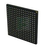
XCV100E-6FGG256C
XCV100E-6FGG256C ECAD Model
XCV100E-6FGG256C Attributes
| Type | Description | Select |
|---|---|---|
| Pbfree Code | Yes | |
| Rohs Code | Yes | |
| Part Life Cycle Code | Obsolete | |
| Supply Voltage-Nom | 1.8 V | |
| Number of Inputs | 176 | |
| Number of Outputs | 176 | |
| Number of Logic Cells | 2700 | |
| Number of Equivalent Gates | 32400 | |
| Number of CLBs | 600 | |
| Combinatorial Delay of a CLB-Max | 470 ps | |
| Programmable Logic Type | FIELD PROGRAMMABLE GATE ARRAY | |
| Temperature Grade | OTHER | |
| Package Shape | SQUARE | |
| Technology | CMOS | |
| Organization | 600 CLBS, 32400 GATES | |
| Clock Frequency-Max | 357 MHz | |
| Power Supplies | 1.2/3.6,1.8 V | |
| Supply Voltage-Max | 1.89 V | |
| Supply Voltage-Min | 1.71 V | |
| JESD-30 Code | S-PBGA-B256 | |
| Qualification Status | Not Qualified | |
| JESD-609 Code | e1 | |
| Moisture Sensitivity Level | 3 | |
| Operating Temperature-Max | 85 °C | |
| Peak Reflow Temperature (Cel) | 260 | |
| Time@Peak Reflow Temperature-Max (s) | 30 | |
| Number of Terminals | 256 | |
| Package Body Material | PLASTIC/EPOXY | |
| Package Code | BGA | |
| Package Equivalence Code | BGA256,16X16,40 | |
| Package Shape | SQUARE | |
| Package Style | GRID ARRAY | |
| Surface Mount | YES | |
| Terminal Finish | Tin/Silver/Copper (Sn95.5Ag4.0Cu0.5) | |
| Terminal Form | BALL | |
| Terminal Pitch | 1 mm | |
| Terminal Position | BOTTOM | |
| Width | 17 mm | |
| Length | 17 mm | |
| Seated Height-Max | 2 mm | |
| Ihs Manufacturer | XILINX INC | |
| Part Package Code | BGA | |
| Package Description | BGA, BGA256,16X16,40 | |
| Pin Count | 256 | |
| Reach Compliance Code | compliant | |
| ECCN Code | EAR99 | |
| HTS Code | 8542.39.00.01 |
XCV100E-6FGG256C Datasheet Download
XCV100E-6FGG256C Overview
The Xilinx XCV100E-6FGG256C is a high-performance, low-cost field programmable gate array (FPGA) chip designed to meet the needs of a wide variety of digital signal processing, embedded processing, and image processing applications. It is a single-chip solution that offers excellent performance and scalability in a small form factor, making it an ideal choice for many applications.
The XCV100E-6FGG256C is designed to be used with the Verilog or VHDL hardware description language (HDL). This allows the user to create custom designs that can be implemented in the FPGA. With the XCV100E-6FGG256C, users are able to create complex designs that can be used for a variety of applications.
The XCV100E-6FGG256C is designed for high-performance digital signal processing, embedded processing, and image processing applications. It is capable of performing complex operations such as convolution and correlation in real time, making it an ideal choice for applications such as radar, sonar, and medical imaging. The XCV100E-6FGG256C is also suitable for advanced communication systems such as cellular, Wi-Fi, and satellite.
The product description of the XCV100E-6FGG256C states that it is a low-cost, low-power, single-chip solution that offers excellent performance and scalability. It has a 256-bit wide data bus, a 256-bit wide configuration port, and a 256-bit wide control port. The XCV100E-6FGG256C also features an integrated memory controller and an integrated clock generator.
In terms of design requirements, the XCV100E-6FGG256C must be programmed using Verilog or VHDL. It must also be configured with a valid configuration bitstream that is compatible with the XCV100E-6FGG256C. The user must also ensure that the design is compatible with the XCV100E-6FGG256C’s internal logic.
There are several case studies and success stories of users who have successfully implemented the XCV100E-6FGG256C in their applications. For example, a team of engineers at a medical imaging company used the XCV100E-6FGG256C to create a real-time image processing system. The system was able to process images in real time, allowing for faster diagnosis and treatment of patients.
When using the XCV100E-6FGG256C, users should take certain precautions. The user must ensure that the design is compatible with the XCV100E-6FGG256C’s internal logic. Additionally, the user must ensure that the configuration bitstream is valid and compatible with the XCV100E-6FGG256C. Finally, the user must ensure that the design does not exceed the XCV100E-6FGG256C’s power and thermal limits.
The Xilinx XCV100E-6FGG256C is a powerful, low-cost FPGA chip that is ideal for a wide range of applications. It is designed to be used with the Verilog or VHDL hardware description language and has a wide range of features that make it an ideal choice for many applications. With the XCV100E-6FGG256C, users can create complex designs that can be used for a variety of applications. Additionally, the XCV100E-6FGG256C is suitable for advanced communication systems and is capable of performing complex operations such as convolution and correlation in real time. However, users must take certain precautions when using the XCV100E-6FGG256C, such as ensuring that the design is compatible with the XCV100E-6FGG256C’s internal logic and that the configuration bitstream is valid and compatible with the XCV100E-6FGG256C.
You May Also Be Interested In
1,789 In Stock
Pricing (USD)
| QTY | Unit Price | Ext Price |
|---|---|---|
| No reference price found. | ||
