AMD Xilinx
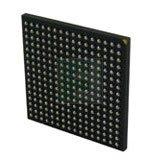
XC2VP4-7FGG256C
XC2VP4-7FGG256C ECAD Model
XC2VP4-7FGG256C Attributes
| Type | Description | Select |
|---|---|---|
| Pbfree Code | Yes | |
| Rohs Code | Yes | |
| Part Life Cycle Code | Obsolete | |
| Supply Voltage-Nom | 1.5 V | |
| Number of Inputs | 140 | |
| Number of Outputs | 140 | |
| Number of Logic Cells | 6768 | |
| Number of CLBs | 752 | |
| Combinatorial Delay of a CLB-Max | 280 ps | |
| Programmable Logic Type | FIELD PROGRAMMABLE GATE ARRAY | |
| Temperature Grade | OTHER | |
| Package Shape | SQUARE | |
| Technology | CMOS | |
| Organization | 752 CLBS | |
| Clock Frequency-Max | 1.35 GHz | |
| Power Supplies | 1.5,1.5/3.3,2/2.5,2.5 V | |
| Supply Voltage-Max | 1.575 V | |
| Supply Voltage-Min | 1.425 V | |
| JESD-30 Code | S-PBGA-B256 | |
| Qualification Status | Not Qualified | |
| JESD-609 Code | e1 | |
| Moisture Sensitivity Level | 3 | |
| Operating Temperature-Max | 85 °C | |
| Peak Reflow Temperature (Cel) | 260 | |
| Time@Peak Reflow Temperature-Max (s) | 30 | |
| Number of Terminals | 256 | |
| Package Body Material | PLASTIC/EPOXY | |
| Package Code | BGA | |
| Package Equivalence Code | BGA256,16X16,40 | |
| Package Shape | SQUARE | |
| Package Style | GRID ARRAY | |
| Surface Mount | YES | |
| Terminal Finish | Tin/Silver/Copper (Sn95.5Ag4.0Cu0.5) | |
| Terminal Form | BALL | |
| Terminal Pitch | 1 mm | |
| Terminal Position | BOTTOM | |
| Width | 17 mm | |
| Length | 17 mm | |
| Seated Height-Max | 2 mm | |
| Ihs Manufacturer | XILINX INC | |
| Part Package Code | BGA | |
| Package Description | BGA, BGA256,16X16,40 | |
| Pin Count | 256 | |
| Reach Compliance Code | compliant | |
| ECCN Code | EAR99 | |
| HTS Code | 8542.39.00.01 |
XC2VP4-7FGG256C Datasheet Download
XC2VP4-7FGG256C Overview
The XC2VP4-7FGG256C chip model is a powerful and versatile tool for digital signal processing, embedded processing, and image processing. It is designed for high-performance applications and requires the use of HDL language. This chip model has several advantages that make it ideal for a variety of applications.
The XC2VP4-7FGG256C chip model is designed with a 7-layer FPGA fabric, allowing for high-speed data processing and routing. It is optimized for power efficiency and supports up to 256 Kbits of embedded RAM and up to 16 Kbits of distributed RAM. It also supports up to 16 user-defined I/O pins and up to 32 user-defined logic blocks. The chip model is also designed to be compatible with a wide range of popular HDL languages, making it easy to integrate into existing systems.
The XC2VP4-7FGG256C chip model is suitable for a wide range of applications, including high-performance digital signal processing, embedded processing, and image processing. It is also well-suited for applications that require high-speed data processing and routing, such as automotive, medical, and industrial automation. The chip model is also suitable for applications that require low power consumption and high performance, such as mobile devices and embedded systems.
When designing a system with the XC2VP4-7FGG256C chip model, it is important to consider the specific design requirements of the application. For example, the chip model supports up to 16 user-defined I/O pins, so the number of pins required for the application should be taken into account. Additionally, the chip model has a maximum clock frequency of 200 MHz, so applications that require higher clock frequencies may require additional design considerations.
The XC2VP4-7FGG256C chip model has been used in a variety of applications, including high-speed imaging systems, 3D printing systems, and industrial automation systems. In each of these cases, the chip model was able to provide the necessary performance and power efficiency while meeting the specific design requirements of the application.
In the future, the demand for the XC2VP4-7FGG256C chip model is expected to continue to grow in a variety of industries. As applications become more complex and require higher performance and lower power consumption, the chip model will be well-suited to meet these requirements. Additionally, as more applications require the use of HDL language, the chip model’s compatibility with a wide range of popular HDL languages will be an invaluable asset.
In conclusion, the XC2VP4-7FGG256C chip model is a powerful and versatile tool for digital signal processing, embedded processing, and image processing. Its advantages make it ideal for a variety of applications, and its compatibility with a wide range of popular HDL languages makes it easy to integrate into existing systems. As applications become more complex and require higher performance and lower power consumption, the chip model is well-suited to meet these requirements. The demand for the XC2VP4-7FGG256C chip model is expected to continue to grow in a variety of industries, and it is an invaluable asset for applications that require the use of HDL language.
You May Also Be Interested In
3,974 In Stock
Pricing (USD)
| QTY | Unit Price | Ext Price |
|---|---|---|
| No reference price found. | ||
