AMD Xilinx
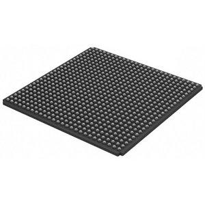
XC2VP30-7FG676I
XC2VP30-7FG676I ECAD Model
XC2VP30-7FG676I Attributes
| Type | Description | Select |
|---|---|---|
| Pbfree Code | No | |
| Rohs Code | No | |
| Part Life Cycle Code | Obsolete | |
| Supply Voltage-Nom | 1.5 V | |
| Number of Inputs | 416 | |
| Number of Outputs | 416 | |
| Number of Logic Cells | 30816 | |
| Number of CLBs | 3424 | |
| Combinatorial Delay of a CLB-Max | 280 ps | |
| Programmable Logic Type | FIELD PROGRAMMABLE GATE ARRAY | |
| Temperature Grade | INDUSTRIAL | |
| Package Shape | SQUARE | |
| Technology | CMOS | |
| Organization | 3424 CLBS | |
| Clock Frequency-Max | 1.35 GHz | |
| Supply Voltage-Max | 1.575 V | |
| Supply Voltage-Min | 1.425 V | |
| JESD-30 Code | S-PBGA-B676 | |
| Qualification Status | Not Qualified | |
| JESD-609 Code | e0 | |
| Moisture Sensitivity Level | 3 | |
| Operating Temperature-Max | 100 °C | |
| Operating Temperature-Min | -40 °C | |
| Peak Reflow Temperature (Cel) | 225 | |
| Time@Peak Reflow Temperature-Max (s) | 30 | |
| Number of Terminals | 676 | |
| Package Body Material | PLASTIC/EPOXY | |
| Package Code | BGA | |
| Package Equivalence Code | BGA676,26X26,40 | |
| Package Shape | SQUARE | |
| Package Style | GRID ARRAY | |
| Surface Mount | YES | |
| Terminal Finish | Tin/Lead (Sn63Pb37) | |
| Terminal Form | BALL | |
| Terminal Pitch | 1 mm | |
| Terminal Position | BOTTOM | |
| Width | 27 mm | |
| Length | 27 mm | |
| Seated Height-Max | 2.6 mm | |
| Ihs Manufacturer | XILINX INC | |
| Part Package Code | BGA | |
| Package Description | 1 MM PITCH, FBGA-676 | |
| Pin Count | 676 | |
| Reach Compliance Code | not_compliant | |
| HTS Code | 8542.39.00.01 |
XC2VP30-7FG676I Datasheet Download
XC2VP30-7FG676I Overview
The XC2VP30-7FG676I chip model is a powerful and versatile solution for high-performance digital signal processing, embedded processing, and image processing. This chip is designed to be programmed using HDL (Hardware Description Language) and offers a wide range of potential applications.
This chip model is ideal for use in networks and intelligent scenarios, as it is designed to handle complex tasks with ease. It is capable of performing advanced machine learning tasks, such as image recognition, natural language processing, and autonomous navigation. It can also be used for a variety of other tasks, such as data analysis, data mining, and artificial intelligence.
The XC2VP30-7FG676I chip model has a number of design requirements that must be taken into consideration. It requires a specific voltage and current range, as well as a specific number of pins. It also has specific timing requirements, which must be met in order for the chip to function properly.
When designing a system using the XC2VP30-7FG676I chip model, it is important to consider the actual case studies and precautions. This includes taking into account the environmental conditions in which the chip will be used, such as temperature and humidity, as well as any potential risks associated with the use of the chip. It is also important to ensure that the design is optimized for the specific application and that all safety protocols are followed.
The XC2VP30-7FG676I chip model is an excellent solution for high-performance digital signal processing, embedded processing, and image processing. It is capable of handling complex tasks and can be used in a variety of networks and intelligent scenarios. With careful consideration of the design requirements and actual case studies, this chip model can be used in the era of fully intelligent systems.
You May Also Be Interested In
4,520 In Stock
Pricing (USD)
| QTY | Unit Price | Ext Price |
|---|---|---|
| No reference price found. | ||
