
AMD Xilinx
XC2VP30-7FFG896I
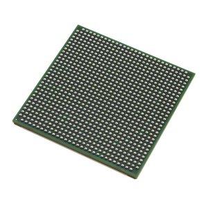
XC2VP30-7FFG896I ECAD Model
XC2VP30-7FFG896I Attributes
| Type | Description | Select |
|---|---|---|
| Pbfree Code | Yes | |
| Rohs Code | Yes | |
| Part Life Cycle Code | Obsolete | |
| Supply Voltage-Nom | 1.5 V | |
| Number of CLBs | 3424 | |
| Combinatorial Delay of a CLB-Max | 280 ps | |
| Programmable Logic Type | FIELD PROGRAMMABLE GATE ARRAY | |
| Package Shape | SQUARE | |
| Technology | CMOS | |
| Organization | 3424 CLBS | |
| Clock Frequency-Max | 1.35 GHz | |
| Supply Voltage-Max | 1.575 V | |
| Supply Voltage-Min | 1.425 V | |
| JESD-30 Code | S-PBGA-B896 | |
| Qualification Status | Not Qualified | |
| JESD-609 Code | e1 | |
| Moisture Sensitivity Level | 4 | |
| Peak Reflow Temperature (Cel) | 245 | |
| Time@Peak Reflow Temperature-Max (s) | 30 | |
| Number of Terminals | 896 | |
| Package Body Material | PLASTIC/EPOXY | |
| Package Code | BGA | |
| Package Shape | SQUARE | |
| Package Style | GRID ARRAY | |
| Surface Mount | YES | |
| Terminal Finish | Tin/Silver/Copper (Sn95.5Ag4.0Cu0.5) | |
| Terminal Form | BALL | |
| Terminal Pitch | 1 mm | |
| Terminal Position | BOTTOM | |
| Width | 31 mm | |
| Length | 31 mm | |
| Seated Height-Max | 3.4 mm | |
| Ihs Manufacturer | XILINX INC | |
| Part Package Code | BGA | |
| Package Description | 1 MM PITCH, FLIP CHIP, FBGA-896 | |
| Pin Count | 896 | |
| Reach Compliance Code | not_compliant | |
| HTS Code | 8542.39.00.01 |
XC2VP30-7FFG896I Datasheet Download
XC2VP30-7FFG896I Overview
The Xilinx XC2VP30-7FFG896I chip model is a powerful and versatile integrated circuit (IC) device that has been designed to meet the needs of a wide range of applications. It is a field programmable gate array (FPGA) device that has been developed to offer high-performance, low-cost, and low-power solutions for a variety of applications. With its advanced features and capabilities, the XC2VP30-7FFG896I chip model is ideal for use in advanced communication systems.
The XC2VP30-7FFG896I chip model incorporates a number of features and functions that make it suitable for a variety of applications. It is designed to provide a high-speed, low-power solution for a variety of communication systems. It has a wide range of programmable logic blocks, including a wide range of memory blocks and configurable logic blocks, which can be used to customize the design of the chip model to meet the specific requirements of the application. It also includes a range of I/O peripherals and a variety of communication protocols, allowing it to be used in a wide range of communication systems.
The XC2VP30-7FFG896I chip model also offers the possibility of future upgrades, allowing the user to upgrade the device to meet the changing needs of their application. The device can also be used in the development and popularization of future intelligent robots, as it is capable of supporting a wide range of communication protocols. In order to use the XC2VP30-7FFG896I chip model effectively, technical personnel should be familiar with the product description and specific design requirements of the device. They should also be aware of the precautions that need to be taken when using the device, as well as the actual case studies that have been conducted with the device.
In conclusion, the XC2VP30-7FFG896I chip model is a powerful and versatile device that can be used in a variety of applications. It offers the possibility of future upgrades, and can be used in the development and popularization of future intelligent robots. In order to use the device effectively, technical personnel should be familiar with the product description and specific design requirements of the device, as well as the actual case studies that have been conducted with the device.
You May Also Be Interested In
2,059 In Stock
Pricing (USD)
| QTY | Unit Price | Ext Price |
|---|---|---|
| No reference price found. | ||