
AMD Xilinx
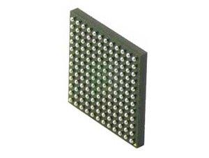
XC2V250-6CSG144I
XC2V250-6CSG144I ECAD Model
XC2V250-6CSG144I Attributes
| Type | Description | Select |
|---|---|---|
| Pbfree Code | Yes | |
| Rohs Code | Yes | |
| Part Life Cycle Code | Obsolete | |
| Supply Voltage-Nom | 1.5 V | |
| Number of Inputs | 92 | |
| Number of Outputs | 92 | |
| Number of Logic Cells | 3456 | |
| Number of Equivalent Gates | 250000 | |
| Number of CLBs | 384 | |
| Combinatorial Delay of a CLB-Max | 350 ps | |
| Programmable Logic Type | FIELD PROGRAMMABLE GATE ARRAY | |
| Package Shape | SQUARE | |
| Technology | CMOS | |
| Organization | 384 CLBS, 250000 GATES | |
| Clock Frequency-Max | 820 MHz | |
| Power Supplies | 1.5,1.5/3.3,3.3 V | |
| Supply Voltage-Max | 1.575 V | |
| Supply Voltage-Min | 1.425 V | |
| JESD-30 Code | S-PBGA-B144 | |
| Qualification Status | Not Qualified | |
| JESD-609 Code | e1 | |
| Moisture Sensitivity Level | 3 | |
| Peak Reflow Temperature (Cel) | 260 | |
| Time@Peak Reflow Temperature-Max (s) | 30 | |
| Number of Terminals | 144 | |
| Package Body Material | PLASTIC/EPOXY | |
| Package Code | TFBGA | |
| Package Equivalence Code | BGA144,13X13,32 | |
| Package Shape | SQUARE | |
| Package Style | GRID ARRAY, THIN PROFILE, FINE PITCH | |
| Surface Mount | YES | |
| Terminal Finish | Tin/Silver/Copper (Sn95.5Ag4.0Cu0.5) | |
| Terminal Form | BALL | |
| Terminal Pitch | 800 µm | |
| Terminal Position | BOTTOM | |
| Width | 12 mm | |
| Length | 12 mm | |
| Seated Height-Max | 1.2 mm | |
| Ihs Manufacturer | XILINX INC | |
| Reach Compliance Code | compliant | |
| HTS Code | 8542.39.00.01 | |
| Part Package Code | BGA | |
| Package Description | TFBGA, BGA144,13X13,32 | |
| Pin Count | 144 |
XC2V250-6CSG144I Datasheet Download
XC2V250-6CSG144I Overview
The XC2V250-6CSG144I is a Field Programmable Gate Array (FPGA) chip model designed to fulfill the requirements of high-performance digital signal processing, embedded processing, image processing, and more. The chip model is designed to be programmed in Hardware Description Language (HDL), allowing developers to customize the chip to their specific needs.
The original design intention of the XC2V250-6CSG144I was to provide a reliable and efficient solution for high-performance digital signal processing, embedded processing, image processing, and more. With its versatile architecture, the chip model is capable of fulfilling the needs of a wide range of applications. Furthermore, the XC2V250-6CSG144I is also capable of being upgraded with additional components, allowing for future expansion.
In terms of product description, the XC2V250-6CSG144I is a single-chip solution with a range of features such as 6,144 logic cells, 8 dedicated Multi-Gigabit Transceivers (MGTs), and a large number of I/O pins. The chip model also features a high-speed memory interface, allowing users to access large amounts of data quickly and efficiently. Additionally, the chip model is designed to be compatible with a wide range of HDL languages, making it suitable for a variety of applications.
In terms of design requirements, the XC2V250-6CSG144I requires a high degree of accuracy and reliability. Developers should take into account the chip model's power consumption, temperature, and other environmental factors when designing their application. Furthermore, developers should also consider the chip model's compatibility with advanced communication systems.
To illustrate the capabilities of the XC2V250-6CSG144I, a number of case studies have been conducted. In one case study, the chip model was used to develop a high-performance image processing system. The system was able to process large amounts of data quickly and efficiently, making it suitable for a range of applications. In another case study, the chip model was used to develop an advanced communication system. The system was able to handle large amounts of data with minimal latency and was able to be integrated with other systems.
In conclusion, the XC2V250-6CSG144I is a versatile and reliable chip model designed to fulfill a wide range of applications. The chip model is capable of being upgraded with additional components and is compatible with a range of HDL languages. Furthermore, the chip model is capable of being used in advanced communication systems, making it suitable for a variety of applications. Developers should take into account the chip model's power consumption, temperature, and other environmental factors when designing their application.
You May Also Be Interested In
2,519 In Stock
Pricing (USD)
| QTY | Unit Price | Ext Price |
|---|---|---|
| No reference price found. | ||