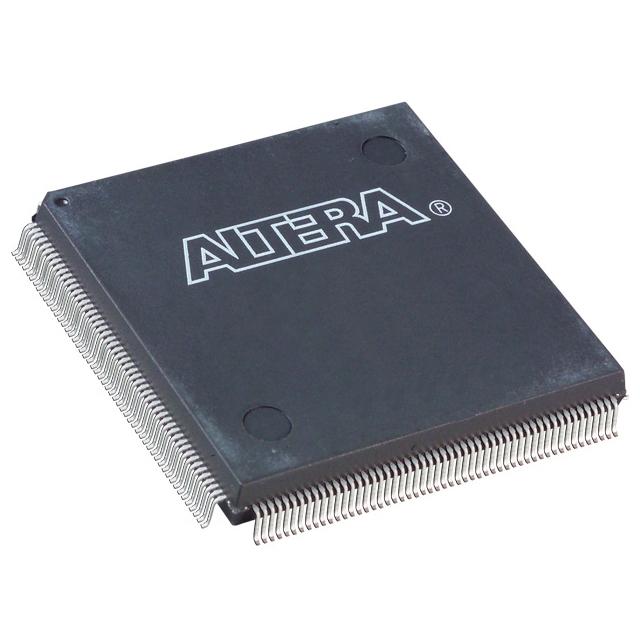
Intel Corporation
EP1K30QI208-2
EP1K30QI208-2 ECAD Model
EP1K30QI208-2 Attributes
| Type | Description | Select |
|---|---|---|
| Mfr | Intel | |
| Series | ACEX-1K® | |
| Package | Tray | |
| Number of LABs/CLBs | 216 | |
| Number of Logic Elements/Cells | 1728 | |
| Total RAM Bits | 24576 | |
| Number of I/O | 147 | |
| Number of Gates | 119000 | |
| Voltage - Supply | 2.375V ~ 2.625V | |
| Mounting Type | Surface Mount | |
| Operating Temperature | 0°C ~ 70°C (TA) | |
| Package / Case | 208-BFQFP | |
| Supplier Device Package | 208-PQFP (28x28) | |
| Base Product Number | EP1K30 |
EP1K30QI208-2 Datasheet Download
EP1K30QI208-2 Overview
The EP1K30QI208-2 is an FPGA (Field Programmable Gate Array) chip from Altera. It is based on the Stratix II architecture and is manufactured using a 0.13-micron CMOS process. The chip has an array of 30,000 logic elements, with a total of 6,000 Kbits of embedded memory. It also includes 10,000 LEs for embedded multipliers and 4,000 LEs for embedded memory blocks.
The chip has a total of 208 I/O pins, with up to 160 user I/O pins, with a maximum I/O voltage of 3.3V. The maximum clock frequency is 200 MHz, and the device has a total power dissipation of 10W. It also has a total of 10 PLLs (Phase Locked Loops).
The EP1K30QI208-2 is suitable for a wide range of applications, including communications, networking, video processing, image processing, and medical imaging. It is also suitable for use in automotive and industrial applications. The device is ideal for applications that require high performance, low power, and high density.
In addition, the device has an integrated JTAG (Joint Test Action Group) port for debugging and programming. It also includes an on-chip trace buffer for debugging, as well as a power-on reset circuit. The EP1K30QI208-2 is available in a variety of packages, including the QFP (Quad Flat Package), BGA (Ball Grid Array), and the PGA (Pin Grid Array).
You May Also Be Interested In
1,560 In Stock
Pricing (USD)
| QTY | Unit Price | Ext Price |
|---|---|---|
| No reference price found. | ||


