
AMD Xilinx
XC2VP7-5FFG896I
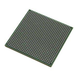
XC2VP7-5FFG896I ECAD Model
XC2VP7-5FFG896I Attributes
| Type | Description | Select |
|---|---|---|
| Pbfree Code | Yes | |
| Rohs Code | Yes | |
| Part Life Cycle Code | Obsolete | |
| Supply Voltage-Nom | 1.5 V | |
| Number of Inputs | 396 | |
| Number of Outputs | 396 | |
| Number of Logic Cells | 11088 | |
| Number of CLBs | 1232 | |
| Combinatorial Delay of a CLB-Max | 360 ps | |
| Programmable Logic Type | FIELD PROGRAMMABLE GATE ARRAY | |
| Package Shape | SQUARE | |
| Technology | CMOS | |
| Organization | 1232 CLBS | |
| Clock Frequency-Max | 1.05 GHz | |
| Power Supplies | 1.5,1.5/3.3,2/2.5,2.5 V | |
| Supply Voltage-Max | 1.575 V | |
| Supply Voltage-Min | 1.425 V | |
| JESD-30 Code | S-PBGA-B896 | |
| Qualification Status | Not Qualified | |
| JESD-609 Code | e1 | |
| Moisture Sensitivity Level | 4 | |
| Peak Reflow Temperature (Cel) | 245 | |
| Time@Peak Reflow Temperature-Max (s) | 30 | |
| Number of Terminals | 896 | |
| Package Body Material | PLASTIC/EPOXY | |
| Package Code | BGA | |
| Package Equivalence Code | BGA896,30X30,40 | |
| Package Shape | SQUARE | |
| Package Style | GRID ARRAY | |
| Surface Mount | YES | |
| Terminal Finish | Tin/Silver/Copper (Sn95.5Ag4.0Cu0.5) | |
| Terminal Form | BALL | |
| Terminal Pitch | 1 mm | |
| Terminal Position | BOTTOM | |
| Width | 31 mm | |
| Length | 31 mm | |
| Seated Height-Max | 3.4 mm | |
| Ihs Manufacturer | XILINX INC | |
| Part Package Code | BGA | |
| Package Description | BGA, BGA896,30X30,40 | |
| Pin Count | 896 | |
| Reach Compliance Code | not_compliant | |
| ECCN Code | 3A991.D | |
| HTS Code | 8542.39.00.01 |
XC2VP7-5FFG896I Datasheet Download
XC2VP7-5FFG896I Overview
The XC2VP7-5FFG896I chip model is a high-performance digital signal processing, embedded processing, and image processing chip that requires the use of HDL language. It is designed to meet the ever-growing demands of the digital world, allowing for faster and more efficient data processing.
The industry trends of the XC2VP7-5FFG896I chip model and the future development of related industries depend on what specific technologies are needed. It is likely that the application environment will require the support of new technologies and the possibility of future upgrades. Advanced communication systems may also require the use of this chip model for their operations.
The original design intention of the XC2VP7-5FFG896I chip model was to provide a high-performance solution for digital signal processing, embedded processing, and image processing. It is designed to provide a reliable and efficient solution for these types of operations. The possibility of future upgrades is also available, allowing for the chip model to be used in more advanced communication systems.
Overall, the XC2VP7-5FFG896I chip model is a great solution for high-performance digital signal processing, embedded processing, and image processing. It is designed to provide a reliable and efficient solution for these types of operations, and is capable of being upgraded to meet the demands of more advanced communication systems. With the right technologies, it is possible to keep up with the ever-changing industry trends and ensure that the chip model remains relevant in the future.
You May Also Be Interested In

2,675 In Stock
Pricing (USD)
| QTY | Unit Price | Ext Price |
|---|---|---|
| 1+ | $260.4003 | $260.4003 |
| 10+ | $257.6003 | $2,576.0028 |
| 100+ | $243.6003 | $24,360.0261 |
| 1000+ | $229.6002 | $114,800.1230 |
| 10000+ | $210.0002 | $210,000.2250 |
| The price is for reference only, please refer to the actual quotation! | ||