
AMD Xilinx
XC2V80-5FGG256C
XC2V80-5FGG256C ECAD Model
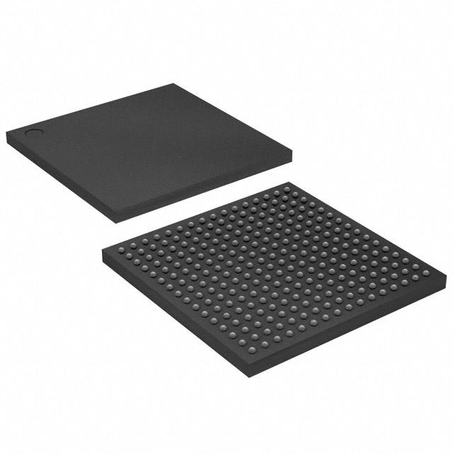
XC2V80-5FGG256C Attributes
| Type | Description | Select |
|---|---|---|
| Mfr | AMD Xilinx | |
| Series | Virtex®-II | |
| Package | Tray | |
| Number of LABs/CLBs | 128 | |
| Total RAM Bits | 147456 | |
| Number of I/O | 120 | |
| Number of Gates | 80000 | |
| Voltage - Supply | 1.425V ~ 1.575V | |
| Mounting Type | Surface Mount | |
| Operating Temperature | 0°C ~ 85°C (TJ) | |
| Package / Case | 256-BGA | |
| Supplier Device Package | 256-FBGA (17x17) | |
| Base Product Number | XC2V80 |
XC2V80-5FGG256C Datasheet Download
XC2V80-5FGG256C Overview
The XC2V80-5FGG256C is a Field Programmable Gate Array (FPGA) chip from Xilinx. It is a high-performance, low-cost, low-power device designed for a variety of applications. It is based on the Virtex-2V architecture and is manufactured using 0.13-micron CMOS technology.
The XC2V80-5FGG256C features 256K system gates, including 8192 logic cells, 8192 flip-flops, and 8192 RAM blocks. It also features a variety of I/O options, including up to 12 LVTTL I/O banks, 8 LVDS I/O banks, and up to 6 clock networks. It has a total of 8 power supply pins and a maximum operating frequency of 200 MHz.
The XC2V80-5FGG256C is suitable for a wide range of applications, such as high-speed data acquisition, image processing, and embedded control. It is also ideal for applications that require a high level of integration, such as communication systems, automotive systems, and industrial automation.
The XC2V80-5FGG256C is a reliable and powerful chip that is suitable for a wide range of applications. It is easy to use and configure, making it an ideal choice for engineers and designers who need a reliable and cost-effective solution.
You May Also Be Interested In
4,966 In Stock
Pricing (USD)
| QTY | Unit Price | Ext Price |
|---|---|---|
| No reference price found. | ||