
AMD Xilinx
XC2V500-5FGG256I
XC2V500-5FGG256I ECAD Model
XC2V500-5FGG256I Attributes
| Type | Description | Select |
|---|---|---|
| Mfr | AMD Xilinx | |
| Series | Virtex®-II | |
| Package | Tray | |
| Number of LABs/CLBs | 768 | |
| Total RAM Bits | 589824 | |
| Number of I/O | 172 | |
| Number of Gates | 500000 | |
| Voltage - Supply | 1.425V ~ 1.575V | |
| Mounting Type | Surface Mount | |
| Operating Temperature | -40°C ~ 100°C (TJ) | |
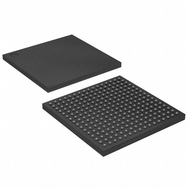
| Package / Case | 256-BGA | |
| Supplier Device Package | 256-FBGA (17x17) | |
| Base Product Number | XC2V500 |
XC2V500-5FGG256I Datasheet Download
XC2V500-5FGG256I Overview
The XC2V500-5FGG256I is a field-programmable gate array (FPGA) chip manufactured by Xilinx Inc. It is a low-cost, low-power, high-performance programmable logic device. It is designed to provide a flexible and cost-effective solution for a wide range of applications.
The XC2V500-5FGG256I is a 5-input/5-output (5F) device with 256 logic cells. It has a total of 1.1 million system gates and is capable of operating at up to 200 MHz. It also features a built-in phase-locked loop (PLL) for clock generation and synchronization. The device is packaged in a 256-pin fine-pitch ball grid array (FBGA) package.
The XC2V500-5FGG256I is suitable for a variety of applications, including embedded systems, networking, communications, industrial automation, medical devices, and consumer electronics. It can be used to implement digital signal processing (DSP) algorithms, logic functions, memory control, and other complex logic functions.
In summary, the XC2V500-5FGG256I is a low-cost, low-power, high-performance programmable logic device that is suitable for a variety of applications. It features 1.1 million system gates, a PLL for clock generation and synchronization, and a 256-pin FBGA package.
You May Also Be Interested In
4,113 In Stock
Pricing (USD)
| QTY | Unit Price | Ext Price |
|---|---|---|
| No reference price found. | ||