
AMD Xilinx
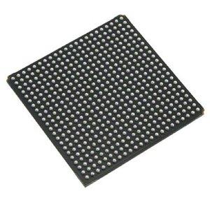
XA3S1400A-4FGG484Q
XA3S1400A-4FGG484Q ECAD Model
XA3S1400A-4FGG484Q Attributes
| Type | Description | Select |
|---|---|---|
| Rohs Code | Yes | |
| Part Life Cycle Code | Active | |
| Supply Voltage-Nom | 1.2 V | |
| Number of Inputs | 375 | |
| Number of Outputs | 288 | |
| Number of Logic Cells | 25344 | |
| Number of Equivalent Gates | 1400000 | |
| Number of CLBs | 2816 | |
| Combinatorial Delay of a CLB-Max | 4.88 ns | |
| Programmable Logic Type | FIELD PROGRAMMABLE GATE ARRAY | |
| Screening Level | AEC-Q100 | |
| Temperature Grade | AUTOMOTIVE | |
| Package Shape | SQUARE | |
| Technology | CMOS | |
| Organization | 2816 CLBS, 1400000 GATES | |
| Clock Frequency-Max | 667 MHz | |
| Power Supplies | 1.2,1.2/3.3,3.3 V | |
| Supply Voltage-Max | 1.26 V | |
| Supply Voltage-Min | 1.14 V | |
| JESD-30 Code | S-PBGA-B484 | |
| Qualification Status | Not Qualified | |
| JESD-609 Code | e1 | |
| Moisture Sensitivity Level | 3 | |
| Operating Temperature-Max | 125 °C | |
| Operating Temperature-Min | -40 °C | |
| Peak Reflow Temperature (Cel) | 250 | |
| Time@Peak Reflow Temperature-Max (s) | 30 | |
| Number of Terminals | 484 | |
| Package Body Material | PLASTIC/EPOXY | |
| Package Code | BGA | |
| Package Equivalence Code | BGA484,22X22,40 | |
| Package Shape | SQUARE | |
| Package Style | GRID ARRAY | |
| Surface Mount | YES | |
| Terminal Finish | TIN SILVER COPPER | |
| Terminal Form | BALL | |
| Terminal Pitch | 1 mm | |
| Terminal Position | BOTTOM | |
| Width | 23 mm | |
| Length | 23 mm | |
| Seated Height-Max | 2.6 mm | |
| Ihs Manufacturer | XILINX INC | |
| Part Package Code | BGA | |
| Package Description | LEAD FREE, MS-034, FGBGA-484 | |
| Pin Count | 484 | |
| Reach Compliance Code | compliant | |
| HTS Code | 8542.39.00.01 | |
| ECCN Code | 3A991.D |
XA3S1400A-4FGG484Q Datasheet Download
XA3S1400A-4FGG484Q Overview
The XA3S1400A-4FGG484Q is a high-performance, low-power field programmable gate array (FPGA) chip designed by Xilinx. It is based on the Xilinx Spartan-3A architecture and is fabricated using a 0.13 micron process. It features a total of 1,400 logic cells and 4,848 flip-flops, with a total of 4,848 I/O pins. It supports up to 16 dedicated clock inputs, and has an operating frequency of up to 400 MHz. It also features an array of digital signal processing (DSP) slices, which enable it to perform complex mathematical operations quickly and accurately.
The XA3S1400A-4FGG484Q is ideal for applications that require high performance, low power consumption and flexibility. It is suitable for use in areas such as communications, industrial automation, medical imaging, consumer electronics and automotive. It is also well-suited for use in embedded systems that require a high-performance, low-power solution.
In addition, the XA3S1400A-4FGG484Q is designed to be compatible with the Xilinx Vivado Design Suite, which provides an integrated design environment for developing FPGA designs. This makes it easy to develop and debug designs quickly and efficiently.
Overall, the XA3S1400A-4FGG484Q is a powerful, low-power FPGA chip that is suitable for a wide range of applications. It provides high performance and flexibility, while also being easy to use with the Xilinx Vivado Design Suite.
You May Also Be Interested In
4,271 In Stock
Pricing (USD)
| QTY | Unit Price | Ext Price |
|---|---|---|
| 1+ | $100.5888 | $100.5888 |
| 10+ | $99.5072 | $995.0720 |
| 100+ | $94.0992 | $9,409.9200 |
| 1000+ | $88.6912 | $44,345.6000 |
| 10000+ | $81.1200 | $81,120.0000 |
| The price is for reference only, please refer to the actual quotation! | ||