

Lattice Semiconductor Corporation
LFXP2-40E-6FN672I
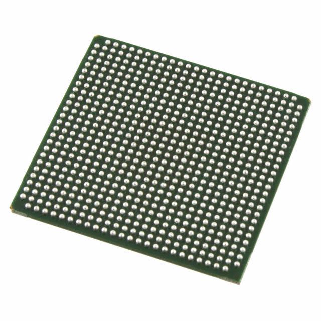
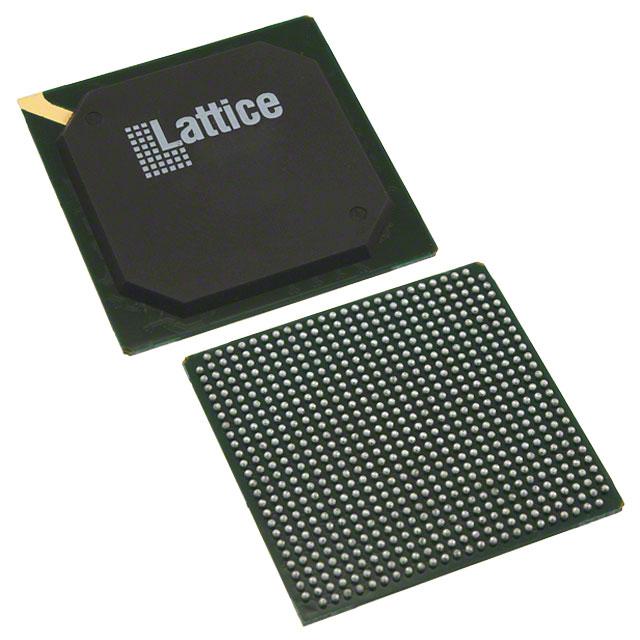
LFXP2-40E-6FN672I ECAD Model
LFXP2-40E-6FN672I Attributes
| Type | Description | Select |
|---|---|---|
| Mfr | Lattice Semiconductor Corporation | |
| Series | XP2 | |
| Package | Tray | |
| Number of LABs/CLBs | 5000 | |
| Number of Logic Elements/Cells | 40000 | |
| Total RAM Bits | 906240 | |
| Number of I/O | 540 | |
| Voltage - Supply | 1.14V ~ 1.26V | |
| Mounting Type | Surface Mount | |
| Operating Temperature | -40°C ~ 100°C (TJ) | |
| Package / Case | 672-BBGA | |
| Supplier Device Package | 672-FPBGA (27x27) | |
| Base Product Number | LFXP2-40 |
LFXP2-40E-6FN672I Datasheet Download
LFXP2-40E-6FN672I Overview
The LFXP2-40E-6FN672I is a low-power, low-voltage field-programmable gate array (FPGA) chip model from Lattice Semiconductor. It is based on the LatticeXP2-40E FPGA architecture, which is designed to provide high system performance and low power consumption. The chip has a total of 6,672 logic cells, distributed across 40Kbits of embedded memory, and can support up to 12,800 logic elements. It also has a total of 8 DSP blocks, each with 48 multipliers, and up to 8,192bits of RAM. The chip operates at a maximum clock frequency of 300MHz and is capable of supporting up to 5.5Gbps of data throughput.
The LFXP2-40E-6FN672I chip model is suitable for a wide variety of applications, such as video processing, image processing, audio processing, communication systems, and embedded systems. It is capable of providing high-speed data processing and supports a wide range of peripherals, including I2C, UART, SPI, and Ethernet. It also has a wide range of I/O capabilities, including LVDS, LVCMOS, and HSTL. The chip is also designed to be power-efficient, with integrated power-saving features such as dynamic voltage scaling and power gating.
Overall, the LFXP2-40E-6FN672I is a low-power, low-voltage FPGA chip model from Lattice Semiconductor that is suitable for a wide range of applications. It has a total of 6,672 logic cells, 8 DSP blocks, and up to 8,192bits of RAM, and can support up to 5.5Gbps of data throughput. It also has a wide range of I/O capabilities, and is designed to be power-efficient.
You May Also Be Interested In
1,154 In Stock
Pricing (USD)
| QTY | Unit Price | Ext Price |
|---|---|---|
| 1+ | $219.3763 | $219.3763 |
| 10+ | $217.0174 | $2,170.1742 |
| 100+ | $205.2230 | $20,522.2995 |
| 1000+ | $193.4286 | $96,714.2850 |
| 10000+ | $176.9164 | $176,916.3750 |
| The price is for reference only, please refer to the actual quotation! | ||