

Lattice Semiconductor Corporation
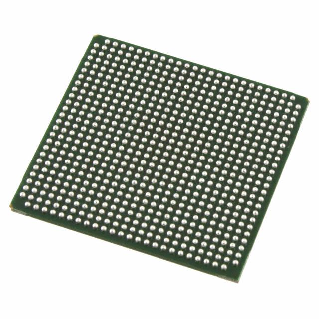
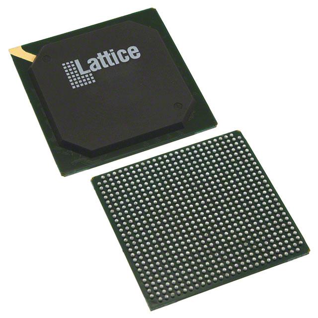
LFXP2-40E-5F672I
LFXP2-40E-5F672I ECAD Model
LFXP2-40E-5F672I Attributes
| Type | Description | Select |
|---|---|---|
| Mfr | Lattice Semiconductor Corporation | |
| Series | XP2 | |
| Package | Tray | |
| Number of LABs/CLBs | 5000 | |
| Number of Logic Elements/Cells | 40000 | |
| Total RAM Bits | 906240 | |
| Number of I/O | 540 | |
| Voltage - Supply | 1.14V ~ 1.26V | |
| Mounting Type | Surface Mount | |
| Operating Temperature | -40°C ~ 100°C (TJ) | |
| Package / Case | 672-BBGA | |
| Supplier Device Package | 672-FPBGA (27x27) | |
| Base Product Number | LFXP2-40 |
LFXP2-40E-5F672I Datasheet Download
LFXP2-40E-5F672I Overview
The LFXP2-40E-5F672I is a low-power, low-cost, small-footprint, field-programmable gate array (FPGA) chip, designed and manufactured by Lattice Semiconductor Corporation. It is based on the LatticeXP2-40E family of FPGAs, and is ideal for applications requiring low cost, low power and small size.
The LFXP2-40E-5F672I FPGA chip has a total of 5,672 logic elements (LEs) and is housed in a 5 x 5mm package. It has an operating voltage range of 1.2V to 3.3V and a maximum operating temperature of up to 105°C. The chip also has a wide range of I/O options, including LVDS, LVCMOS, SPI and I2C as well as a PLL for clock frequency multiplication.
The LFXP2-40E-5F672I FPGA chip is suitable for a wide range of applications, including industrial and medical devices, consumer electronics, automotive, aerospace, and communications. It is also suitable for applications such as motor control, power management, data acquisition, and digital signal processing.
The LFXP2-40E-5F672I FPGA chip offers a low cost, low power, and small size solution for a variety of applications. It is easy to use, and offers a wide range of features and benefits, making it an ideal choice for designers who need a reliable and cost effective FPGA solution.
You May Also Be Interested In
5,730 In Stock
Pricing (USD)
| QTY | Unit Price | Ext Price |
|---|---|---|
| No reference price found. | ||