

Lattice Semiconductor Corporation
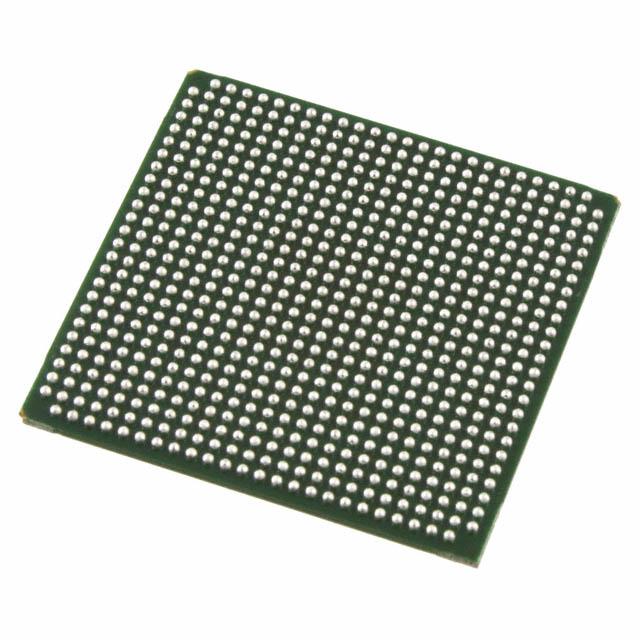
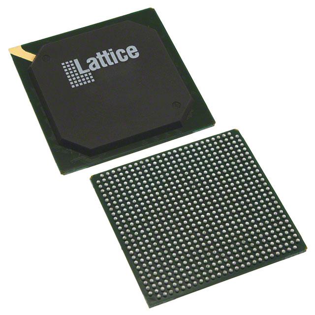
LFXP2-40E-5F672C
LFXP2-40E-5F672C ECAD Model
LFXP2-40E-5F672C Attributes
| Type | Description | Select |
|---|---|---|
| Mfr | Lattice Semiconductor Corporation | |
| Series | XP2 | |
| Package | Tray | |
| Number of LABs/CLBs | 5000 | |
| Number of Logic Elements/Cells | 40000 | |
| Total RAM Bits | 906240 | |
| Number of I/O | 540 | |
| Voltage - Supply | 1.14V ~ 1.26V | |
| Mounting Type | Surface Mount | |
| Operating Temperature | 0°C ~ 85°C (TJ) | |
| Package / Case | 672-BBGA | |
| Supplier Device Package | 672-FPBGA (27x27) | |
| Base Product Number | LFXP2-40 |
LFXP2-40E-5F672C Datasheet Download
LFXP2-40E-5F672C Overview
The LFXP2-40E-5F672C is a low-power, low-cost, field-programmable, mixed-signal integrated circuit (IC) from the Lattice Semiconductor Corporation. It is a member of the LatticeXP2 family of FPGAs (Field Programmable Gate Arrays).
The LFXP2-40E-5F672C features 5,672 logic cells, 32Kbits of RAM, and up to 400 I/O pins. It has a total power dissipation of 2.2W, and operates at a maximum frequency of 300MHz. Its core voltage is 1.2V, and its I/O voltage is 3.3V. Its temperature range is from -40°C to 85°C, and it has a maximum clock-to-out delay of 4.5ns. It also features a wide range of I/O standards, including LVDS, LVCMOS, and SGMII.
The LFXP2-40E-5F672C is suitable for a wide range of applications, including embedded systems, communications, industrial automation, medical, automotive, and military applications. It is also suitable for use in high-speed networking applications, such as 10/100/1000 Ethernet, 10 Gigabit Ethernet, and Fibre Channel.
The LFXP2-40E-5F672C is a reliable, cost-effective solution for a variety of applications. Its low power consumption and wide range of I/O standards make it an ideal choice for a variety of projects.
You May Also Be Interested In
5,582 In Stock
Pricing (USD)
| QTY | Unit Price | Ext Price |
|---|---|---|
| No reference price found. | ||