
Lattice Semiconductor Corporation
LFSC3GA80E-5FFN1152C
LFSC3GA80E-5FFN1152C ECAD Model
LFSC3GA80E-5FFN1152C Attributes
| Type | Description | Select |
|---|---|---|
| Mfr | Lattice Semiconductor Corporation | |
| Series | SC | |
| Package | Tray | |
| Number of LABs/CLBs | 20000 | |
| Number of Logic Elements/Cells | 80000 | |
| Total RAM Bits | 5816320 | |
| Number of I/O | 660 | |
| Voltage - Supply | 0.95V ~ 1.26V | |
| Mounting Type | Surface Mount | |
| Operating Temperature | 0°C ~ 85°C (TJ) | |
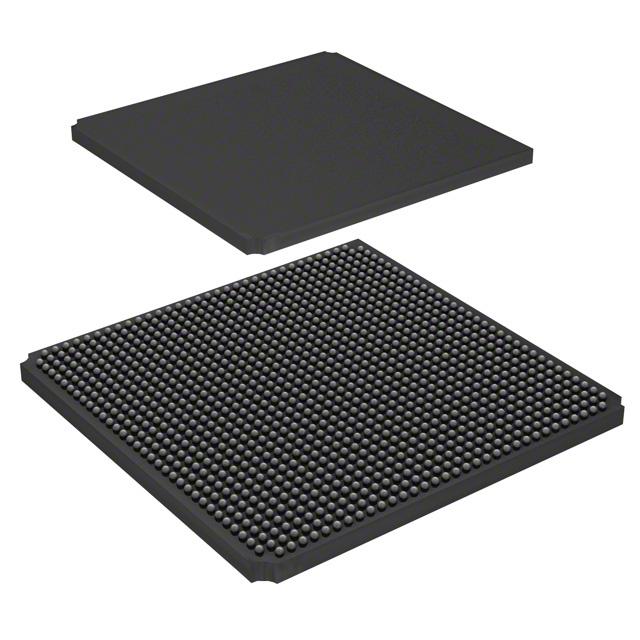
| Package / Case | 1152-BBGA | |
| Supplier Device Package | 1152-FPBGA (35x35) | |
| Base Product Number | LFSC3GA80 |
LFSC3GA80E-5FFN1152C Datasheet Download
LFSC3GA80E-5FFN1152C Overview
The LFSC3GA80E-5FFN1152C is an advanced, low-power, high-performance Field Programmable Gate Array (FPGA) chip manufactured by Lattice Semiconductor. It is based on the Lattice FPGA architecture and is designed to provide a cost-effective solution for a wide range of applications.
The LFSC3GA80E-5FFN1152C chip features a large capacity of 80K logic elements, 624 I/O pins, and a maximum clock frequency of 250 MHz. It is powered by a 3.3V power supply and has a maximum power consumption of 4.5W. It also includes a variety of features such as dynamic power management, adaptive logic technology, and programmable interconnects.
The LFSC3GA80E-5FFN1152C is suitable for a wide range of applications including automotive, industrial, medical, consumer, and communication systems. It can be used for a variety of functions such as digital signal processing, data acquisition, image processing, system control and monitoring, and more.
The LFSC3GA80E-5FFN1152C chip is highly reliable and offers superior performance. It is also compatible with a variety of development tools, making it easy to program and debug. The chip also offers a wide range of features that make it suitable for a variety of applications.
You May Also Be Interested In
3,770 In Stock
Pricing (USD)
| QTY | Unit Price | Ext Price |
|---|---|---|
| No reference price found. | ||