
Lattice Semiconductor Corporation
LFE2M70SE-6F1152I
LFE2M70SE-6F1152I ECAD Model
LFE2M70SE-6F1152I Attributes
| Type | Description | Select |
|---|---|---|
| Mfr | Lattice Semiconductor Corporation | |
| Series | ECP2M | |
| Package | Tray | |
| Number of LABs/CLBs | 8375 | |
| Number of Logic Elements/Cells | 67000 | |
| Total RAM Bits | 4642816 | |
| Number of I/O | 436 | |
| Voltage - Supply | 1.14V ~ 1.26V | |
| Mounting Type | Surface Mount | |
| Operating Temperature | -40°C ~ 100°C (TJ) | |
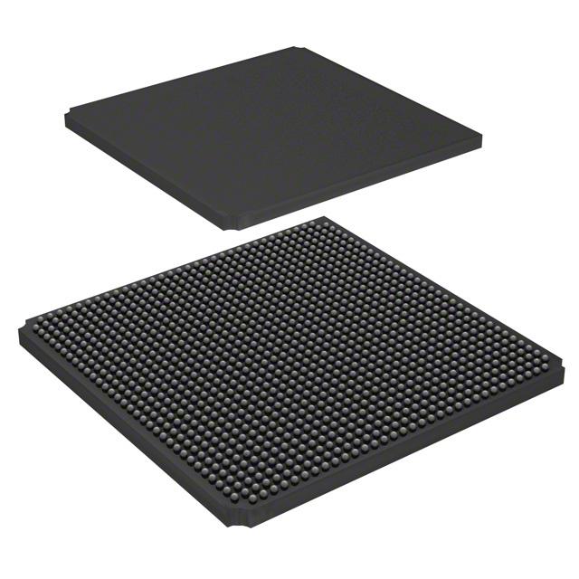
| Package / Case | 1152-BBGA | |
| Supplier Device Package | 1152-FPBGA (35x35) | |
| Base Product Number | LFE2M70 |
LFE2M70SE-6F1152I Datasheet Download
LFE2M70SE-6F1152I Overview
The LFE2M70SE-6F1152I is a Field Programmable Gate Array (FPGA) from Lattice Semiconductor. It is a low-cost, low-power, high-performance FPGA that can be used for a variety of applications. It has a total of 70K logic elements, 152 I/O pins, and 4Mbits of on-chip RAM. It is designed to be used in a variety of applications such as industrial automation, robotics, medical imaging, and consumer electronics.
The LFE2M70SE-6F1152I is built on a low-power, low-cost, and highly reliable 28nm process technology. It has a maximum operating frequency of up to 350MHz and a maximum operating temperature range of -40°C to +125°C. It also has an integrated phase-locked loop (PLL) for clock synchronization, as well as a range of I/O interfaces, including LVDS, LVCMOS, and SERDES.
The LFE2M70SE-6F1152I supports a wide range of advanced features, including high-speed DDR3 and DDR4 memory interfaces, PCIe Gen3, Ethernet, USB 3.0, and SATA. It also includes a range of security features such as secure boot, secure key storage, and secure debug.
In summary, the LFE2M70SE-6F1152I is a low-cost, low-power, high-performance FPGA from Lattice Semiconductor. It is built on a 28nm process technology and has a maximum operating frequency of up to 350MHz. It has a total of 70K logic elements, 152 I/O pins, and 4Mbits of on-chip RAM. It is designed for a variety of applications, including industrial automation, robotics, medical imaging, and consumer electronics. It supports a wide range of advanced features, including high-speed DDR3 and DDR4 memory interfaces, PCIe Gen3, Ethernet, USB 3.0, and SATA.
You May Also Be Interested In
2,497 In Stock
Pricing (USD)
| QTY | Unit Price | Ext Price |
|---|---|---|
| 1+ | $354.0919 | $354.0919 |
| 10+ | $350.2845 | $3,502.8448 |
| 100+ | $331.2473 | $33,124.7280 |
| 1000+ | $312.2101 | $156,105.0400 |
| 10000+ | $285.5580 | $285,558.0000 |
| The price is for reference only, please refer to the actual quotation! | ||