
Lattice Semiconductor Corporation
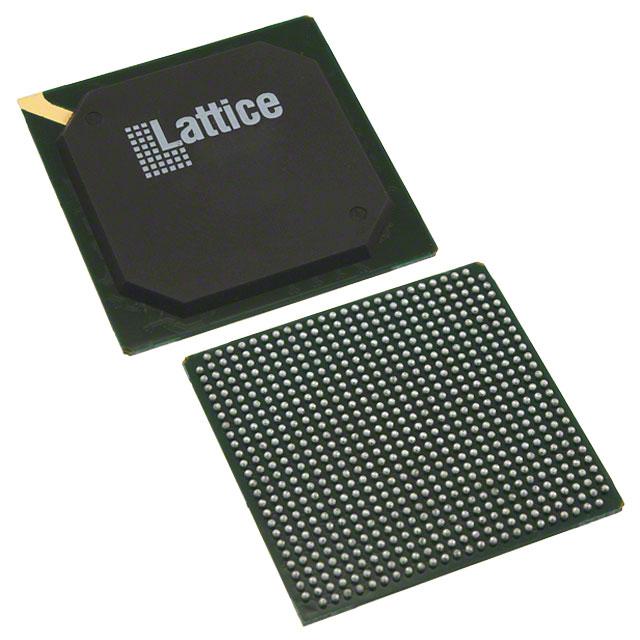
LFECP33E-3FN672I
LFECP33E-3FN672I ECAD Model
LFECP33E-3FN672I Attributes
| Type | Description | Select |
|---|---|---|
| Mfr | Lattice Semiconductor Corporation | |
| Series | ECP | |
| Package | Tray | |
| Number of Logic Elements/Cells | 32800 | |
| Total RAM Bits | 434176 | |
| Number of I/O | 496 | |
| Voltage - Supply | 1.14V ~ 1.26V | |
| Mounting Type | Surface Mount | |
| Operating Temperature | -40°C ~ 100°C (TJ) | |
| Package / Case | 672-BBGA | |
| Supplier Device Package | 672-FPBGA (27x27) | |
| Base Product Number | LFECP33 |
LFECP33E-3FN672I Datasheet Download
LFECP33E-3FN672I Overview
The LFECP33E-3FN672I is a low-power, highly integrated, low-cost Field Programmable Gate Array (FPGA) from Lattice Semiconductor. It is based on the LatticeECP3 FPGA architecture, which offers high performance, low power consumption and scalability. The device features 3.3V I/O, 672 user I/O pins, and up to 33K logic elements. It is capable of delivering up to 800MHz performance in a wide range of applications.
The device provides a range of features, such as high-speed SERDES, DDR2/DDR3/QDRII/QDRII+/RLDRAM memory interfaces, up to 8 PLLs, up to 8 DSP blocks and up to 4 Multi Gigabit Transceivers (MGTs). It also includes a range of embedded peripherals, such as SPI, I2C, UART, CAN, and GPIO.
The LFECP33E-3FN672I is suitable for a wide range of applications, including industrial automation, medical devices, automotive, communications, consumer, and military/aerospace. It is also suitable for applications such as digital signal processing, image processing, high-speed communications, and high-speed networking.
The device is available in a range of packages, including a 484-pin BGA, a 384-pin BGA, and a 256-pin BGA. It is also RoHS compliant and meets the requirements of the European Union's Restriction of Hazardous Substances (RoHS) directive.
You May Also Be Interested In
1,882 In Stock
Pricing (USD)
| QTY | Unit Price | Ext Price |
|---|---|---|
| No reference price found. | ||