
Lattice Semiconductor Corporation
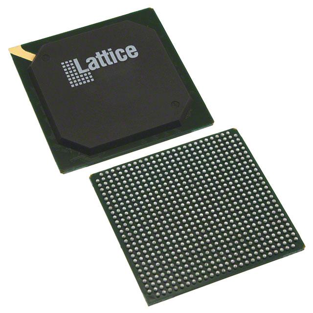
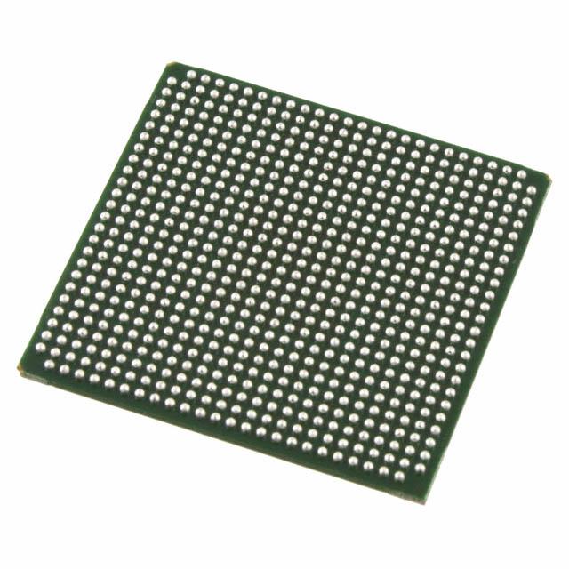
LFECP33E-3FN672C
LFECP33E-3FN672C ECAD Model
LFECP33E-3FN672C Attributes
| Type | Description | Select |
|---|---|---|
| Mfr | Lattice Semiconductor Corporation | |
| Series | ECP | |
| Package | Tray | |
| Number of Logic Elements/Cells | 32800 | |
| Total RAM Bits | 434176 | |
| Number of I/O | 496 | |
| Voltage - Supply | 1.14V ~ 1.26V | |
| Mounting Type | Surface Mount | |
| Operating Temperature | 0°C ~ 85°C (TJ) | |
| Package / Case | 672-BBGA | |
| Supplier Device Package | 672-FPBGA (27x27) | |
| Base Product Number | LFECP33 |
LFECP33E-3FN672C Datasheet Download
LFECP33E-3FN672C Overview
The LFECP33E-3FN672C is a low-power, low-voltage field-programmable gate array (FPGA) chip designed by Lattice Semiconductor. It is a member of the MachXO3 family and is based on the LatticeECP3 architecture. The chip has a 672-pin FineLine BGA package, with a power supply voltage of 1.2V and an operating temperature range of -40°C to +85°C.
The chip has a maximum operating frequency of up to 500 MHz, and a maximum internal power dissipation of 1.5W. It has a maximum of 8,192 logic cells, and a maximum of 1,024 Kb of embedded memory. It also has up to 8 PLLs and over 1,000 I/O pins.
The LFECP33E-3FN672C is suitable for a wide range of applications, such as industrial automation and control, communications, consumer electronics, medical devices, and automotive. It offers features such as low power consumption, low cost, and high reliability, and is ideal for applications that require low power, low cost, and high performance.
The chip also offers advanced features such as an efficient, low-power design, high-speed I/O, and a comprehensive security suite. It is also compatible with a wide range of development tools, such as the Lattice Diamond and ispLEVER software suites, which make it easy to design, configure, and program the chip.
You May Also Be Interested In
5,989 In Stock
Pricing (USD)
| QTY | Unit Price | Ext Price |
|---|---|---|
| No reference price found. | ||