
Lattice Semiconductor Corporation
LFE2M70SE-5FN1152I
LFE2M70SE-5FN1152I ECAD Model
LFE2M70SE-5FN1152I Attributes
| Type | Description | Select |
|---|---|---|
| Mfr | Lattice Semiconductor Corporation | |
| Series | ECP2M | |
| Package | Tray | |
| Number of LABs/CLBs | 8375 | |
| Number of Logic Elements/Cells | 67000 | |
| Total RAM Bits | 4642816 | |
| Number of I/O | 436 | |
| Voltage - Supply | 1.14V ~ 1.26V | |
| Mounting Type | Surface Mount | |
| Operating Temperature | -40°C ~ 100°C (TJ) | |
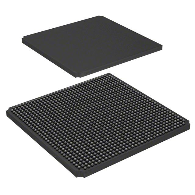
| Package / Case | 1152-BBGA | |
| Supplier Device Package | 1152-FPBGA (35x35) | |
| Base Product Number | LFE2M70 |
LFE2M70SE-5FN1152I Datasheet Download
LFE2M70SE-5FN1152I Overview
The LFE2M70SE-5FN1152I chip model is a low-power, low-cost, high-speed FPGA (Field Programmable Gate Array) designed by Lattice Semiconductor. This device is based on the LatticeECP2M architecture and is suitable for a wide range of applications, including automotive, industrial, telecom, medical, and consumer.
The LFE2M70SE-5FN1152I chip has a maximum operating frequency of up to 500 MHz and can support up to 1536 logic elements. It comes with up to 1.2 million system gates and up to 216 Kbits of embedded memory. It has a total of 1152 I/O pins and supports up to four banks of global clock networks. It also includes a dedicated JTAG port for programming and debugging.
In terms of power consumption, the LFE2M70SE-5FN1152I chip has a typical power consumption of 1.2W and a maximum power consumption of 1.5W. It is also designed for low-power operation with a low-power mode and a power-down mode.
The LFE2M70SE-5FN1152I chip is suitable for a wide range of applications, including industrial automation, medical, automotive, telecom, consumer, and aerospace. It is capable of supporting a variety of interfaces, including Ethernet, PCI Express, USB, and Serial RapidIO. It can also be used for embedded systems, signal processing, video processing, and image processing.
Overall, the LFE2M70SE-5FN1152I chip is a low-cost, low-power, high-speed FPGA device suitable for a wide range of applications. It has a maximum operating frequency of up to 500 MHz and can support up to 1536 logic elements. It also has a total of 1152 I/O pins and supports up to four banks of global clock networks. In terms of power consumption, the device has a typical power consumption of 1.2W and a maximum power consumption of 1.5W. It is also designed for low-power operation with a low-power mode and a power-down mode.
You May Also Be Interested In
4,157 In Stock
Pricing (USD)
| QTY | Unit Price | Ext Price |
|---|---|---|
| 1+ | $260.1284 | $260.1284 |
| 10+ | $257.3314 | $2,573.3136 |
| 100+ | $243.3460 | $24,334.5960 |
| 1000+ | $229.3606 | $114,680.2800 |
| 10000+ | $209.7810 | $209,781.0000 |
| The price is for reference only, please refer to the actual quotation! | ||