
Lattice Semiconductor Corporation
LFE2M70E-5F1152I
LFE2M70E-5F1152I ECAD Model
LFE2M70E-5F1152I Attributes
| Type | Description | Select |
|---|---|---|
| Mfr | Lattice Semiconductor Corporation | |
| Series | ECP2M | |
| Package | Tray | |
| Number of LABs/CLBs | 8375 | |
| Number of Logic Elements/Cells | 67000 | |
| Total RAM Bits | 4642816 | |
| Number of I/O | 436 | |
| Voltage - Supply | 1.14V ~ 1.26V | |
| Mounting Type | Surface Mount | |
| Operating Temperature | -40°C ~ 100°C (TJ) | |
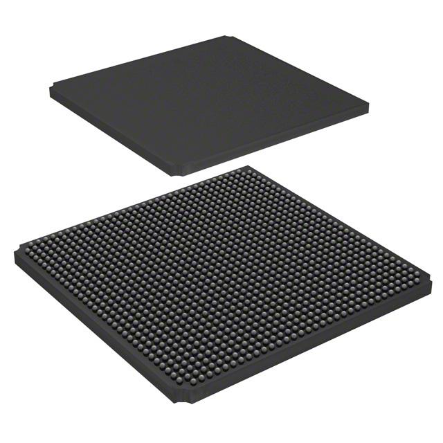
| Package / Case | 1152-BBGA | |
| Supplier Device Package | 1152-FPBGA (35x35) | |
| Base Product Number | LFE2M70 |
LFE2M70E-5F1152I Datasheet Download
LFE2M70E-5F1152I Overview
The LFE2M70E-5F1152I is an FPGA chip from the Lattice Semi product family. It is a low-cost, low-power, and low-density FPGA that is ideal for applications requiring low-cost, low-power solutions. It has a total of 8,192 logic elements, and has a total of 11,520 flip-flops. It also features an internal clock multiplier and an internal PLL for clock synthesis.
The chip is built using a 0.18 um CMOS process and has an operating voltage of 1.2V. It has a maximum operating frequency of 250MHz, and a total of 12 I/O banks, each with a maximum of 128 I/O pins. The chip also features a variety of memory blocks, including RAM, ROM, and registers.
The LFE2M70E-5F1152I is suitable for a wide range of applications, including embedded systems, consumer electronics, automotive, industrial, and communication systems. It is ideal for applications such as image processing, motor control, and system control. The chip is also suitable for use in FPGA-based system-on-chip designs, providing a low-cost, low-power solution for embedded systems.
You May Also Be Interested In
1,520 In Stock
Pricing (USD)
| QTY | Unit Price | Ext Price |
|---|---|---|
| 1+ | $286.1461 | $286.1461 |
| 10+ | $283.0693 | $2,830.6928 |
| 100+ | $267.6851 | $26,768.5080 |
| 1000+ | $252.3009 | $126,150.4400 |
| 10000+ | $230.7630 | $230,763.0000 |
| The price is for reference only, please refer to the actual quotation! | ||