
Lattice Semiconductor Corporation
LFE2M50SE-6FN900I
LFE2M50SE-6FN900I ECAD Model
LFE2M50SE-6FN900I Attributes
| Type | Description | Select |
|---|---|---|
| Mfr | Lattice Semiconductor Corporation | |
| Series | ECP2M | |
| Package | Tray | |
| Number of LABs/CLBs | 6000 | |
| Number of Logic Elements/Cells | 48000 | |
| Total RAM Bits | 4246528 | |
| Number of I/O | 410 | |
| Voltage - Supply | 1.14V ~ 1.26V | |
| Mounting Type | Surface Mount | |
| Operating Temperature | -40°C ~ 100°C (TJ) | |
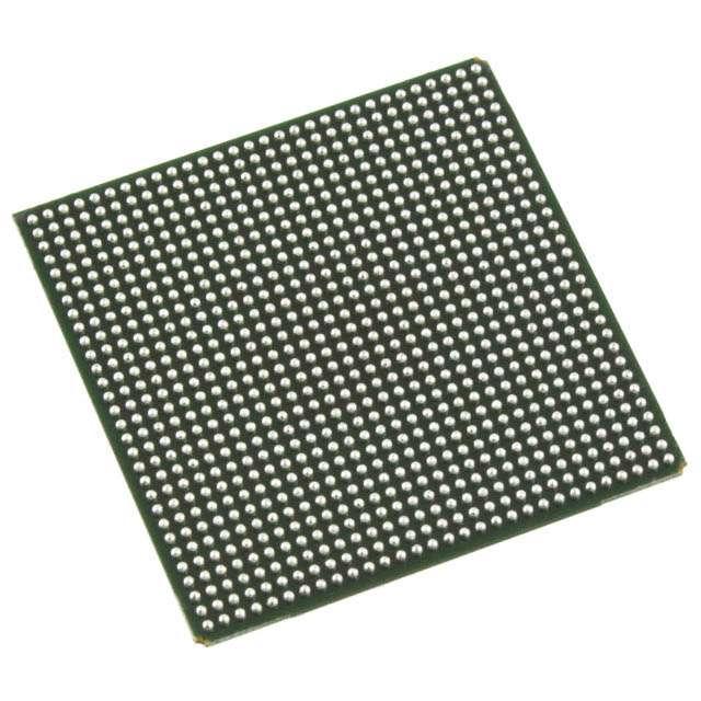
| Package / Case | 900-BBGA | |
| Supplier Device Package | 900-FPBGA (31x31) | |
| Base Product Number | LFE2M50 |
LFE2M50SE-6FN900I Datasheet Download
LFE2M50SE-6FN900I Overview
The LFE2M50SE-6FN900I is a high performance, low power, field programmable gate array (FPGA) chip manufactured by Lattice Semiconductor. The chip is designed to provide a low cost, high performance solution for a wide range of applications. It features a 6-layer metal stack, with up to 900 I/O pins, and a total of 1.3 million logic elements. The chip has an operating voltage range of 1.2V to 3.3V, and a maximum clock frequency of 350MHz. It also features a wide range of memory, DSP, and I/O blocks, as well as on-chip power management circuitry.
The chip is suitable for a wide range of applications, including embedded systems, communications, industrial automation, automotive, and consumer electronics. It can be used for high speed data processing, data acquisition, signal processing, and control applications. The chip also supports a range of communication protocols, including Ethernet, USB, and CAN.
The chip is also designed for reliability, with built-in ESD protection, power-on reset, and a wide range of safety features. It is also designed to be highly configurable, with a wide range of configurable I/O, memory, and DSP blocks. The chip is also designed to be easily integrated into existing systems, with a wide range of development tools and libraries available.
Overall, the LFE2M50SE-6FN900I is a high performance, low power, field programmable gate array (FPGA) chip that is suitable for a wide range of applications, including embedded systems, communications, industrial automation, automotive, and consumer electronics. It features a 6-layer metal stack, up to 900 I/O pins, and a total of 1.3 million logic elements, and is designed for reliability, configurability, and ease of integration.
You May Also Be Interested In
4,712 In Stock
Pricing (USD)
| QTY | Unit Price | Ext Price |
|---|---|---|
| 1+ | $204.2663 | $204.2663 |
| 10+ | $202.0699 | $2,020.6990 |
| 100+ | $191.0878 | $19,108.7844 |
| 1000+ | $180.1058 | $90,052.8920 |
| 10000+ | $164.7309 | $164,730.9000 |
| The price is for reference only, please refer to the actual quotation! | ||