
Lattice Semiconductor Corporation
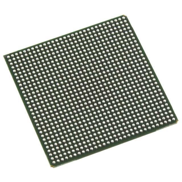
LFE2M50SE-6FN900C
LFE2M50SE-6FN900C ECAD Model
LFE2M50SE-6FN900C Attributes
| Type | Description | Select |
|---|---|---|
| Mfr | Lattice Semiconductor Corporation | |
| Series | ECP2M | |
| Package | Tray | |
| Number of LABs/CLBs | 6000 | |
| Number of Logic Elements/Cells | 48000 | |
| Total RAM Bits | 4246528 | |
| Number of I/O | 410 | |
| Voltage - Supply | 1.14V ~ 1.26V | |
| Mounting Type | Surface Mount | |
| Operating Temperature | 0°C ~ 85°C (TJ) | |
| Package / Case | 900-BBGA | |
| Supplier Device Package | 900-FPBGA (31x31) | |
| Base Product Number | LFE2M50 |
LFE2M50SE-6FN900C Datasheet Download
LFE2M50SE-6FN900C Overview
The LFE2M50SE-6FN900C is a low-power, low-cost, field-programmable gate array (FPGA) chip from Lattice Semiconductor. It is designed for applications such as industrial automation, consumer electronics, and embedded systems. The chip is based on the LatticeECP2M architecture and is built on a 0.6-micron process. It has a total of 50 million system gates and is capable of operating at up to 300MHz.
The chip features up to 9,000 usable logic elements, up to 300Kbits of embedded memory, up to 576 I/Os, and up to four 3.3V PLLs. It also supports both LVDS and LVCMOS I/O standards. It has a total power consumption of up to 1.6W and a maximum operating temperature of 85°C.
The chip is suitable for a wide range of applications, including industrial automation, consumer electronics, and embedded systems. It can be used to develop a variety of products, including programmable logic controllers, motor control systems, digital signal processors, and embedded systems. Additionally, it is also suitable for applications such as communications, networking, and data storage.
In summary, the LFE2M50SE-6FN900C is a low-power, low-cost FPGA chip from Lattice Semiconductor. It is based on the LatticeECP2M architecture and is built on a 0.6-micron process. It has a total of 50 million system gates and is capable of operating at up to 300MHz. It is suitable for a wide range of applications, including industrial automation, consumer electronics, and embedded systems.
You May Also Be Interested In
4,631 In Stock
Pricing (USD)
| QTY | Unit Price | Ext Price |
|---|---|---|
| 1+ | $225.0032 | $225.0032 |
| 10+ | $222.5838 | $2,225.8379 |
| 100+ | $210.4868 | $21,048.6843 |
| 1000+ | $198.3899 | $99,194.9490 |
| 10000+ | $181.4542 | $181,454.1750 |
| The price is for reference only, please refer to the actual quotation! | ||