
Lattice Semiconductor Corporation
LFE2M50SE-5F900C
LFE2M50SE-5F900C ECAD Model
LFE2M50SE-5F900C Attributes
| Type | Description | Select |
|---|---|---|
| Mfr | Lattice Semiconductor Corporation | |
| Series | ECP2M | |
| Package | Tray | |
| Number of LABs/CLBs | 6000 | |
| Number of Logic Elements/Cells | 48000 | |
| Total RAM Bits | 4246528 | |
| Number of I/O | 410 | |
| Voltage - Supply | 1.14V ~ 1.26V | |
| Mounting Type | Surface Mount | |
| Operating Temperature | 0°C ~ 85°C (TJ) | |
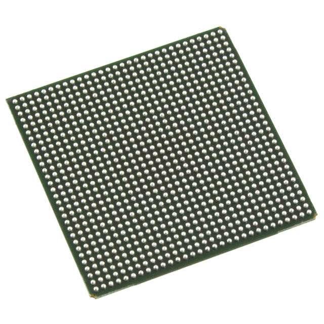
| Package / Case | 900-BBGA | |
| Supplier Device Package | 900-FPBGA (31x31) | |
| Base Product Number | LFE2M50 |
LFE2M50SE-5F900C Datasheet Download
LFE2M50SE-5F900C Overview
The LFE2M50SE-5F900C is a Field Programmable Gate Array (FPGA) chip model manufactured by Lattice Semiconductor Corporation. It is based on the LatticeECP2M FPGA architecture and is available in a 5mm x 5mm, 68-pin, Fine Line BGA package. It has a total of 8,000 logic elements, 8,000 flip-flops, and up to 4,000 4-input look-up tables. It also has embedded high-performance DSP blocks, high-speed SERDES I/O blocks, and up to 166 user I/O pins.
The chip is designed to operate at a maximum speed of 500 MHz and has a maximum power dissipation of 2.6W. It supports a wide range of I/O protocols including DDR2, DDR3, LVDS, and GbE. It also features a wide variety of features such as wide-range voltage support, I/O bank voltage control, and I/O bank power optimization.
The LFE2M50SE-5F900C is suitable for a wide range of applications including industrial, automotive, medical, and aerospace. It can be used in applications such as motion control, motor control, communications, video processing, and image processing. It is also suitable for applications where low power and small form factor are important. The chip is also compliant with the JEDEC standards and is RoHS-compliant.
You May Also Be Interested In
3,492 In Stock
Pricing (USD)
| QTY | Unit Price | Ext Price |
|---|---|---|
| No reference price found. | ||