
Lattice Semiconductor Corporation
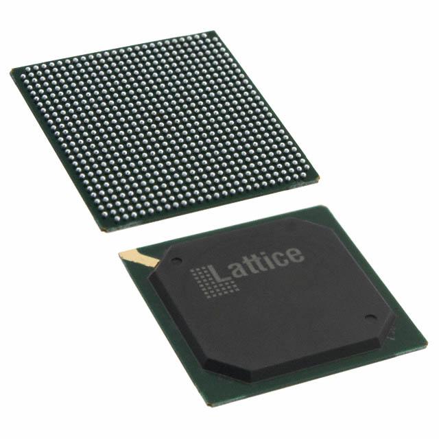
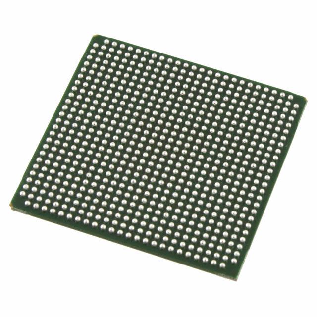
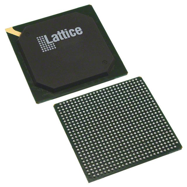
LFE2M50E-6F672I
LFE2M50E-6F672I ECAD Model
LFE2M50E-6F672I Attributes
| Type | Description | Select |
|---|---|---|
| Mfr | Lattice Semiconductor Corporation | |
| Series | ECP2M | |
| Package | Tray | |
| Number of LABs/CLBs | 6000 | |
| Number of Logic Elements/Cells | 48000 | |
| Total RAM Bits | 4246528 | |
| Number of I/O | 372 | |
| Voltage - Supply | 1.14V ~ 1.26V | |
| Mounting Type | Surface Mount | |
| Operating Temperature | -40°C ~ 100°C (TJ) | |
| Package / Case | 672-BBGA | |
| Supplier Device Package | 672-FPBGA (27x27) | |
| Base Product Number | LFE2M50 |
LFE2M50E-6F672I Datasheet Download
LFE2M50E-6F672I Overview
The LFE2M50E-6F672I is a low-power, high-performance FPGA chip model manufactured by Lattice Semiconductor. It is based on the Lattice FPGA architecture and is built on a 6.7 nm process technology. It features a wide variety of configurable logic blocks, memory blocks, and I/O blocks. It also has an embedded processor, high-speed transceivers, and various other components.
The LFE2M50E-6F672I offers up to 150K logic elements, up to 200Kbits of RAM, and up to 1.6Mbits of embedded block RAM. It also provides up to 16 high-speed transceivers with data rates up to 28Gbps. It has a wide variety of I/O standards including LVDS, LVCMOS, and HSTL. The chip also has a wide range of power management features, including dynamic voltage and frequency scaling, power-down modes, and on-chip power management.
The LFE2M50E-6F672I is suitable for a wide range of applications, including industrial automation, automotive, aerospace, and medical. It can be used in wireless communication systems, networking, and computer vision applications. Additionally, it can be used in data acquisition, signal processing, and machine learning applications. The chip is also suitable for use in embedded systems, robotics, and Internet of Things (IoT) applications.
You May Also Be Interested In
3,379 In Stock
Pricing (USD)
| QTY | Unit Price | Ext Price |
|---|---|---|
| No reference price found. | ||