
Lattice Semiconductor Corporation
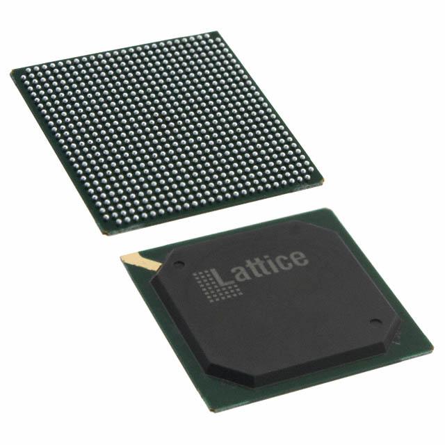
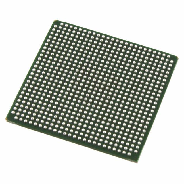
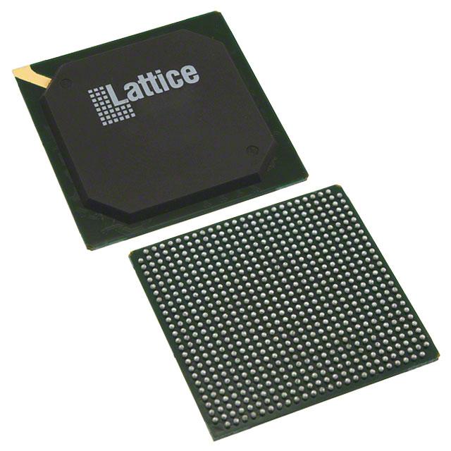
LFE2M35SE-7F672C
LFE2M35SE-7F672C ECAD Model
LFE2M35SE-7F672C Attributes
| Type | Description | Select |
|---|---|---|
| Mfr | Lattice Semiconductor Corporation | |
| Series | ECP2M | |
| Package | Tray | |
| Number of LABs/CLBs | 4250 | |
| Number of Logic Elements/Cells | 34000 | |
| Total RAM Bits | 2151424 | |
| Number of I/O | 410 | |
| Voltage - Supply | 1.14V ~ 1.26V | |
| Mounting Type | Surface Mount | |
| Operating Temperature | 0°C ~ 85°C (TJ) | |
| Package / Case | 672-BBGA | |
| Supplier Device Package | 672-FPBGA (27x27) | |
| Base Product Number | LFE2M35 |
LFE2M35SE-7F672C Datasheet Download
LFE2M35SE-7F672C Overview
The LFE2M35SE-7F672C is a low-power field-programmable gate array (FPGA) from Lattice Semiconductor. It is a cost-effective, low-power, and low-cost FPGA solution for a wide range of applications. The device features a low-power, low-cost architecture with a total power consumption of just 2.5W. It comes with a range of features such as a high-speed, low-latency, and low-power design. It also has a variety of configurable I/O options, including LVDS, LVCMOS, and USB.
The device is based on the LatticeECP3 FPGA family and is designed for a wide range of applications. It is suitable for a variety of embedded applications such as industrial, automotive, and medical. It is also suitable for applications such as image processing, video processing, and communication systems.
The device has a total of 7,672 logic cells, which are divided into four banks. The device also has two banks of SRAM, which provide up to 128KB of memory. It also has two banks of I/O, which provide up to 88 I/O pins. The device has a maximum clock frequency of 350MHz and a maximum operating temperature of 105°C.
The device is also equipped with a range of features to simplify FPGA design. It includes an on-chip JTAG interface, a high-speed serializer/deserializer, and a range of IP cores and peripherals. It also has a range of development tools and support to help designers get the most out of their designs.
Overall, the LFE2M35SE-7F672C is a cost-effective, low-power, and low-cost FPGA solution for a wide range of applications. It is suitable for a variety of embedded applications and can be used in a variety of applications such as image processing, video processing, and communication systems.
You May Also Be Interested In
4,100 In Stock
Pricing (USD)
| QTY | Unit Price | Ext Price |
|---|---|---|
| No reference price found. | ||