
Lattice Semiconductor Corporation
LFE2M100SE-7F900C
LFE2M100SE-7F900C ECAD Model
LFE2M100SE-7F900C Attributes
| Type | Description | Select |
|---|---|---|
| Mfr | Lattice Semiconductor Corporation | |
| Series | ECP2M | |
| Package | Tray | |
| Number of LABs/CLBs | 11875 | |
| Number of Logic Elements/Cells | 95000 | |
| Total RAM Bits | 5435392 | |
| Number of I/O | 416 | |
| Voltage - Supply | 1.14V ~ 1.26V | |
| Mounting Type | Surface Mount | |
| Operating Temperature | 0°C ~ 85°C (TJ) | |
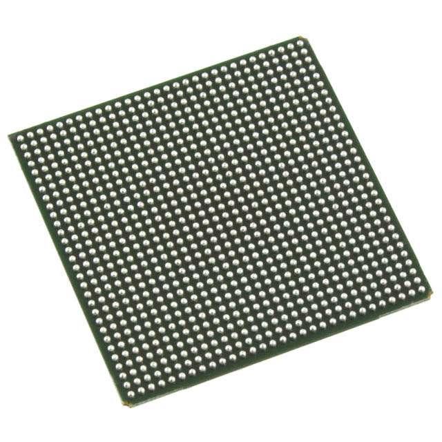
| Package / Case | 900-BBGA | |
| Supplier Device Package | 900-FPBGA (31x31) | |
| Base Product Number | LFE2M100 |
LFE2M100SE-7F900C Datasheet Download
LFE2M100SE-7F900C Overview
The LFE2M100SE-7F900C is an advanced FPGA chip from Lattice Semiconductor. It is a low-power, low-cost FPGA with enhanced features and performance. The chip is based on the LatticeECP2/M architecture and is fabricated using advanced 90nm CMOS technology.
The chip has a total of 4,096 logic cells and 4,096 flip-flops. It also offers a wide range of configurable I/O options with up to 144 user I/Os, two 2.5V LVDS pairs and one 3.3V LVDS pair. The chip also has two high-speed SERDES channels and supports up to four clock domains. It also includes a dedicated JTAG port for programming and debugging.
The chip has an operating voltage range of 0.9V to 1.2V and a maximum power dissipation of 1.5W. It has a maximum operating frequency of 500MHz and a maximum clock frequency of 200MHz. The chip is also RoHS compliant and is available in a 7x7mm, 144-pin BGA package.
The LFE2M100SE-7F900C is ideal for applications such as industrial automation, medical imaging, communications, and consumer electronics. It is also suitable for low-power, low-cost applications such as handheld devices, wearables, and IoT devices.
You May Also Be Interested In
4,140 In Stock
Pricing (USD)
| QTY | Unit Price | Ext Price |
|---|---|---|
| No reference price found. | ||