
Lattice Semiconductor Corporation
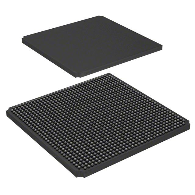
LFE2M100SE-6FN1152I
LFE2M100SE-6FN1152I ECAD Model
LFE2M100SE-6FN1152I Attributes
| Type | Description | Select |
|---|---|---|
| Mfr | Lattice Semiconductor Corporation | |
| Series | ECP2M | |
| Package | Tray | |
| Number of LABs/CLBs | 11875 | |
| Number of Logic Elements/Cells | 95000 | |
| Total RAM Bits | 5435392 | |
| Number of I/O | 520 | |
| Voltage - Supply | 1.14V ~ 1.26V | |
| Mounting Type | Surface Mount | |
| Operating Temperature | -40°C ~ 100°C (TJ) | |
| Package / Case | 1152-BBGA | |
| Supplier Device Package | 1152-FPBGA (35x35) | |
| Base Product Number | LFE2M100 |
LFE2M100SE-6FN1152I Datasheet Download
LFE2M100SE-6FN1152I Overview
The LFE2M100SE-6FN1152I is an advanced Field Programmable Gate Array (FPGA) chip, manufactured by Lattice Semiconductor. It is a low-cost, low-power device, with a maximum power consumption of 1.2W. It features a total of 1,152 logic elements, and has a total of 1.2Mbits of embedded RAM. It offers a wide range of on-chip features, including clock management, on-chip debugging, and advanced I/O support.
The LFE2M100SE-6FN1152I is designed for use in a variety of applications, including embedded systems, automotive, industrial, and consumer electronics. It supports a wide range of I/O protocols, including LVDS, LVCMOS, and SSTL. It also offers a wide range of clock management features, such as clock synthesis, clock gating, and clock domain crossing.
The LFE2M100SE-6FN1152I is also designed to be used in a range of applications, including high-speed networking, video processing, and medical imaging. It is designed to be used in a wide range of temperature ranges, from -40°C to +85°C. It also offers a wide range of on-chip diagnostic features, such as boundary scan, JTAG, and embedded self-test.
In conclusion, the LFE2M100SE-6FN1152I is a low-cost, low-power FPGA chip, designed for use in a variety of applications. It features a total of 1,152 logic elements and 1.2Mbits of embedded RAM, and supports a wide range of I/O protocols. It also offers a wide range of clock management features, and is designed to be used in a range of temperature ranges.
You May Also Be Interested In
4,673 In Stock
Pricing (USD)
| QTY | Unit Price | Ext Price |
|---|---|---|
| 1+ | $530.5092 | $530.5092 |
| 10+ | $524.8048 | $5,248.0480 |
| 100+ | $496.2828 | $49,628.2800 |
| 1000+ | $467.7608 | $233,880.4000 |
| 10000+ | $427.8300 | $427,830.0000 |
| The price is for reference only, please refer to the actual quotation! | ||