

Lattice Semiconductor Corporation
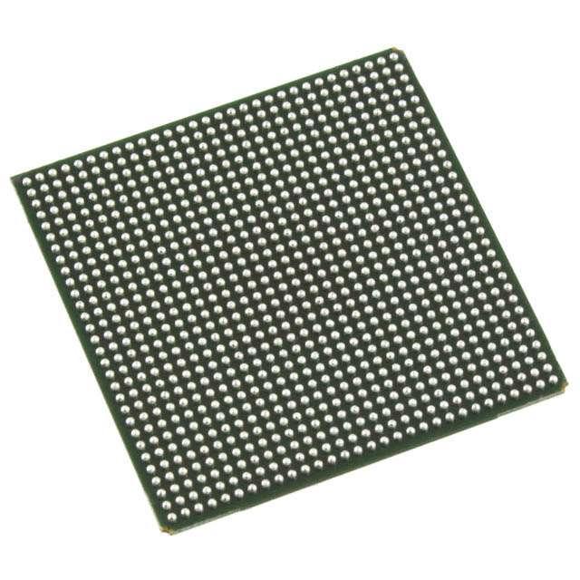
LFE2-70E-6FN900C
LFE2-70E-6FN900C ECAD Model
LFE2-70E-6FN900C Attributes
| Type | Description | Select |
|---|---|---|
| Mfr | Lattice Semiconductor Corporation | |
| Series | ECP2 | |
| Package | Tray | |
| Number of LABs/CLBs | 8500 | |
| Number of Logic Elements/Cells | 68000 | |
| Total RAM Bits | 1056768 | |
| Number of I/O | 583 | |
| Voltage - Supply | 1.14V ~ 1.26V | |
| Mounting Type | Surface Mount | |
| Operating Temperature | 0°C ~ 85°C (TJ) | |
| Package / Case | 900-BBGA | |
| Supplier Device Package | 900-FPBGA (31x31) | |
| Base Product Number | LFE2-70 |
LFE2-70E-6FN900C Datasheet Download
LFE2-70E-6FN900C Overview
The LFE2-70E-6FN900C is a low-power, low-voltage FPGA chip from Lattice Semiconductor. It is a member of the Lattice E2 family, which offers high performance and low power consumption. The chip is built with a 6-layer metal programmable logic array and has a maximum operating frequency of up to 300 MHz. It has 900Kbits of embedded memory and is capable of supporting up to 36K logic elements. The chip also has a wide range of I/O capabilities, including LVDS, SPI, I2C and UART.
The chip is suitable for a wide range of applications, including industrial, automotive, medical, aerospace and consumer electronics. It is designed to be used in embedded systems and can be used to create a variety of designs, including digital signal processing, control systems, data conversion, image processing and more. It also supports multiple development tools and is compatible with a variety of programming languages, including Verilog, VHDL and SystemVerilog.
The chip is designed to be power efficient and offers a wide range of power saving features, such as dynamic voltage scaling, clock gating and power-down modes. It also has a wide range of features for debugging and test, including boundary scan, JTAG and FPGA configuration. The chip also has a wide range of built-in security features, such as secure boot and secure storage.
Overall, the LFE2-70E-6FN900C is an advanced FPGA chip that can be used for a wide range of applications. It offers high performance and low power consumption, along with a wide range of features and development tools. It can be used to create a variety of designs and is suitable for a wide range of industries.
You May Also Be Interested In
5,825 In Stock
Pricing (USD)
| QTY | Unit Price | Ext Price |
|---|---|---|
| 1+ | $243.1599 | $243.1599 |
| 10+ | $240.5453 | $2,405.4532 |
| 100+ | $227.4722 | $22,747.2201 |
| 1000+ | $214.3991 | $107,199.5430 |
| 10000+ | $196.0967 | $196,096.7250 |
| The price is for reference only, please refer to the actual quotation! | ||