
Lattice Semiconductor Corporation
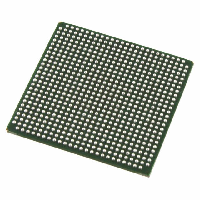
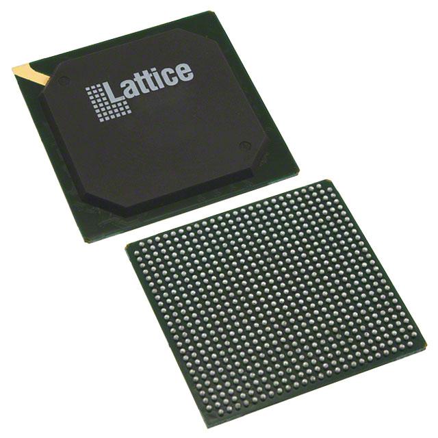
LFE2-50SE-6F672I
LFE2-50SE-6F672I ECAD Model
LFE2-50SE-6F672I Attributes
| Type | Description | Select |
|---|---|---|
| Mfr | Lattice Semiconductor Corporation | |
| Series | ECP2 | |
| Package | Tray | |
| Number of LABs/CLBs | 6000 | |
| Number of Logic Elements/Cells | 48000 | |
| Total RAM Bits | 396288 | |
| Number of I/O | 500 | |
| Voltage - Supply | 1.14V ~ 1.26V | |
| Mounting Type | Surface Mount | |
| Operating Temperature | -40°C ~ 100°C (TJ) | |
| Package / Case | 672-BBGA | |
| Supplier Device Package | 672-FPBGA (27x27) | |
| Base Product Number | LFE2-50 |
LFE2-50SE-6F672I Datasheet Download
LFE2-50SE-6F672I Overview
The LFE2-50SE-6F672I chip model is a low-power, low-cost, field programmable gate array (FPGA) developed by Lattice Semiconductor. This device is designed to provide high performance, low power, and low cost solutions for a wide range of applications. It features 6,672 logic cells, up to 50Kbits of embedded SRAM, up to 4Kbits of embedded Flash memory, and up to 2,400 user-defined I/O pins. It also supports a wide range of I/O standards, including LVDS, RSDS, and LVCMOS.
This FPGA is ideal for applications such as embedded systems, industrial automation, medical imaging, and instrumentation. It is also suitable for use in digital signal processing, communication, and networking applications. This device is available in a variety of packages, including BGA, QFN, and TQFP. It is also available in a variety of speed grades, from -3 to -8.
The LFE2-50SE-6F672I offers a powerful combination of features and performance at a low cost. It is designed to provide excellent performance and power efficiency in a wide range of applications. Its low power consumption and low cost make it ideal for cost-sensitive applications. It is also easy to use and program, making it a great choice for embedded systems and other applications.
You May Also Be Interested In
1,052 In Stock
Pricing (USD)
| QTY | Unit Price | Ext Price |
|---|---|---|
| No reference price found. | ||