
Lattice Semiconductor Corporation
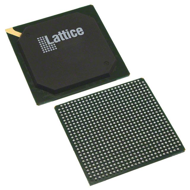
LFE2-50SE-5F672C
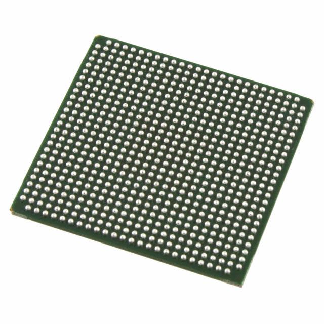
LFE2-50SE-5F672C ECAD Model
LFE2-50SE-5F672C Attributes
| Type | Description | Select |
|---|---|---|
| Mfr | Lattice Semiconductor Corporation | |
| Series | ECP2 | |
| Package | Tray | |
| Number of LABs/CLBs | 6000 | |
| Number of Logic Elements/Cells | 48000 | |
| Total RAM Bits | 396288 | |
| Number of I/O | 500 | |
| Voltage - Supply | 1.14V ~ 1.26V | |
| Mounting Type | Surface Mount | |
| Operating Temperature | 0°C ~ 85°C (TJ) | |
| Package / Case | 672-BBGA | |
| Supplier Device Package | 672-FPBGA (27x27) | |
| Base Product Number | LFE2-50 |
LFE2-50SE-5F672C Datasheet Download
LFE2-50SE-5F672C Overview
The LFE2-50SE-5F672C is a low-power, low-voltage, field-programmable gate array (FPGA) chip developed by Lattice Semiconductor. It is based on the company's low-power, low-voltage LatticeECP2/M FPGA architecture and is optimized for low-power, low-cost, and low-voltage applications.
The chip features a total of 5,672 logic cells, each of which consists of two 4-input look-up tables (LUTs) and two flip-flops. It also has a total of 1,824 Kbits of RAM, 1,024 Kbits of distributed RAM, and 4,096 bits of distributed ROM. The chip also has a total of 576 I/O pins, with up to four banks of I/O pins available.
The chip is designed to operate at a maximum speed of 250 MHz and a maximum supply voltage of 1.2V. It has a wide range of features, including phase-locked loops (PLLs), clock management blocks (CMBs), and embedded memory blocks (EMBs).
The LFE2-50SE-5F672C is suitable for a wide range of applications, including consumer electronics, automotive, industrial, medical, and aerospace. It is particularly well-suited for applications that require low-power, low-cost, and low-voltage operation.
You May Also Be Interested In
2,358 In Stock
Pricing (USD)
| QTY | Unit Price | Ext Price |
|---|---|---|
| No reference price found. | ||