
Lattice Semiconductor Corporation
LFE2-35SE-5FN672C
LFE2-35SE-5FN672C ECAD Model
LFE2-35SE-5FN672C Attributes
| Type | Description | Select |
|---|---|---|
| Mfr | Lattice Semiconductor Corporation | |
| Series | ECP2 | |
| Package | Tray | |
| Number of LABs/CLBs | 4000 | |
| Number of Logic Elements/Cells | 32000 | |
| Total RAM Bits | 339968 | |
| Number of I/O | 450 | |
| Voltage - Supply | 1.14V ~ 1.26V | |
| Mounting Type | Surface Mount | |
| Operating Temperature | 0°C ~ 85°C (TJ) | |
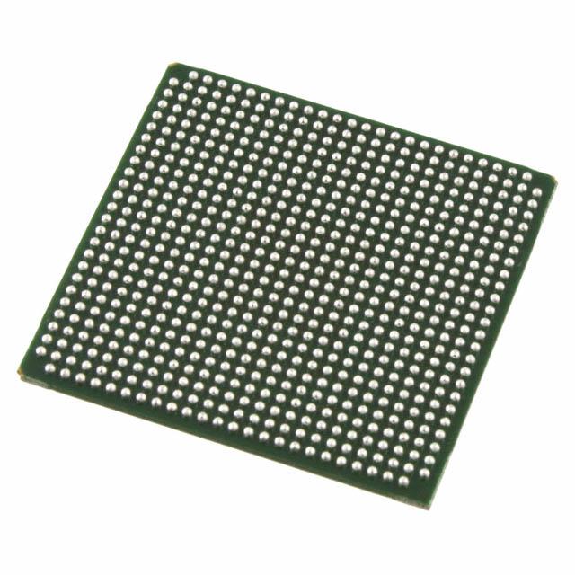
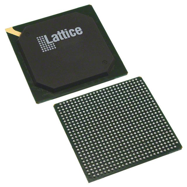
| Package / Case | 672-BBGA | |
| Supplier Device Package | 672-FPBGA (27x27) | |
| Base Product Number | LFE2-35 |
LFE2-35SE-5FN672C Datasheet Download
LFE2-35SE-5FN672C Overview
The LFE2-35SE-5FN672C is an advanced low-power, low-voltage field-programmable gate array (FPGA) chip from Lattice Semiconductor. It is designed for use in high-performance and low-power applications. The chip has a 576-pin Fine-Pitch Ball Grid Array (FBGA) package and is fabricated using a 0.35um CMOS process.
The chip features 35K logic elements, up to 4.2Mbits of embedded memory, up to 1.6Mbits of RAM, and up to 1.6Mbits of ROM. It also includes an embedded microcontroller with an 8-bit RISC processor, 16Kbytes of SRAM, and up to 256Kbytes of Flash memory. The chip also supports up to 32 user-defined I/Os, up to 64 user-defined logic elements, and up to 4 user-defined DSP blocks.
The chip is suitable for a wide range of applications, including communications, consumer, industrial, automotive, and medical. It can be used for applications such as image processing, data acquisition, system control, and embedded systems. It is also suitable for applications that require low power consumption and high performance.
The LFE2-35SE-5FN672C is an advanced low-power, low-voltage FPGA chip from Lattice Semiconductor. It is designed for high-performance and low-power applications, and is suitable for a wide range of applications. It features 35K logic elements, up to 4.2Mbits of embedded memory, up to 1.6Mbits of RAM, and up to 1.6Mbits of ROM, as well as an embedded microcontroller. It also supports up to 32 user-defined I/Os, up to 64 user-defined logic elements, and up to 4 user-defined DSP blocks. Its 576-pin Fine-Pitch Ball Grid Array (FBGA) package is fabricated using a 0.35um CMOS process.
You May Also Be Interested In
5,032 In Stock
Pricing (USD)
| QTY | Unit Price | Ext Price |
|---|---|---|
| 1+ | $106.4815 | $106.4815 |
| 10+ | $105.3365 | $1,053.3650 |
| 100+ | $99.6117 | $9,961.1694 |
| 1000+ | $93.8869 | $46,943.4420 |
| 10000+ | $85.8722 | $85,872.1500 |
| The price is for reference only, please refer to the actual quotation! | ||