
Lattice Semiconductor Corporation
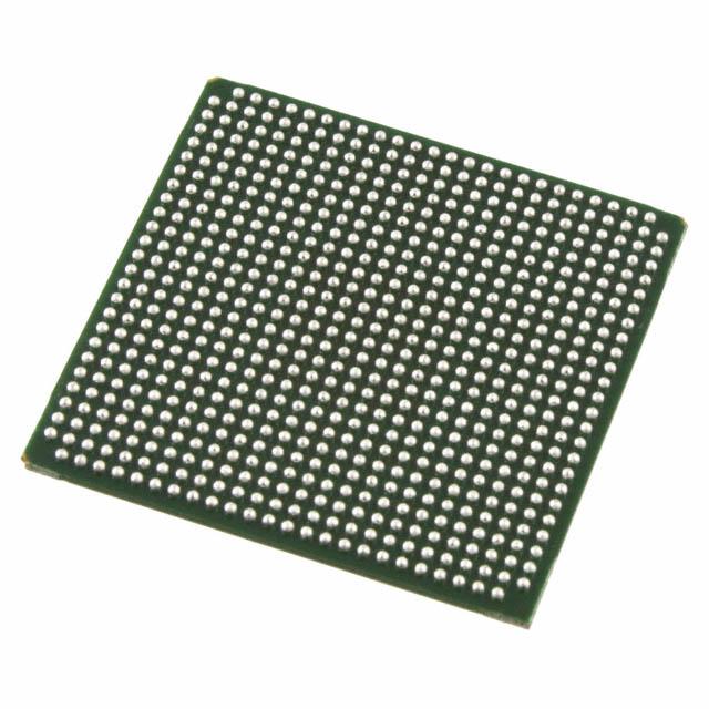
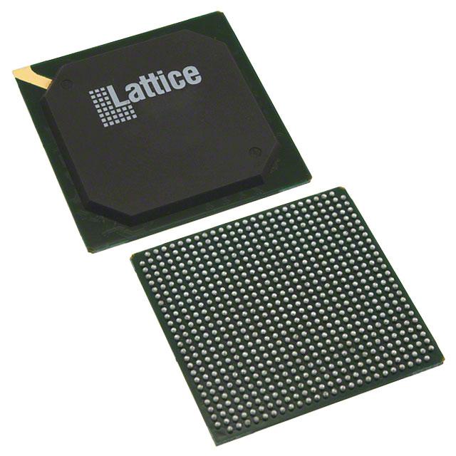
LFE2-35E-6F672I
LFE2-35E-6F672I ECAD Model
LFE2-35E-6F672I Attributes
| Type | Description | Select |
|---|---|---|
| Mfr | Lattice Semiconductor Corporation | |
| Series | ECP2 | |
| Package | Tray | |
| Number of LABs/CLBs | 4000 | |
| Number of Logic Elements/Cells | 32000 | |
| Total RAM Bits | 339968 | |
| Number of I/O | 450 | |
| Voltage - Supply | 1.14V ~ 1.26V | |
| Mounting Type | Surface Mount | |
| Operating Temperature | -40°C ~ 100°C (TJ) | |
| Package / Case | 672-BBGA | |
| Supplier Device Package | 672-FPBGA (27x27) | |
| Base Product Number | LFE2-35 |
LFE2-35E-6F672I Datasheet Download
LFE2-35E-6F672I Overview
The LFE2-35E-6F672I is a Field Programmable Gate Array (FPGA) chip from Lattice Semiconductor. It is a low-power device, with a low-cost, low-power, and low-noise design. It is a 65nm, 6-bit FPGA, with a total of 35,000 logic elements and 6,672 I/O pins. It has a maximum clock frequency of 200 MHz and a power consumption of 0.9 W.
The chip is designed for a variety of applications, including communications, consumer electronics, industrial, medical, and automotive. It features a wide range of features, such as embedded memory, high-speed serial transceivers, and high-speed I/O. It also supports a variety of protocols, such as PCI Express, DDR3, and USB 3.0.
The chip is ideal for applications such as image processing, video processing, networking, and embedded systems. It can be used for both high-speed and low-power applications, and it is well suited for applications that require a high level of flexibility and scalability.
The chip is also designed for use in a variety of operating systems, such as Windows, Linux, and Mac OS. It is also compatible with a variety of development tools, including the Xilinx Vivado Design Suite and the Altera Quartus II Design Suite.
Overall, the LFE2-35E-6F672I is an ideal FPGA chip for a variety of applications. It offers a low-cost, low-power, and low-noise design, and it is well-suited for applications requiring a high level of flexibility and scalability. It is also compatible with a variety of operating systems and development tools, making it an ideal choice for a wide range of applications.
You May Also Be Interested In
1,515 In Stock
Pricing (USD)
| QTY | Unit Price | Ext Price |
|---|---|---|
| 1+ | $112.1952 | $112.1952 |
| 10+ | $110.9888 | $1,109.8880 |
| 100+ | $104.9568 | $10,495.6800 |
| 1000+ | $98.9248 | $49,462.4000 |
| 10000+ | $90.4800 | $90,480.0000 |
| The price is for reference only, please refer to the actual quotation! | ||