
Lattice Semiconductor Corporation
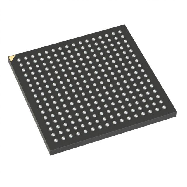
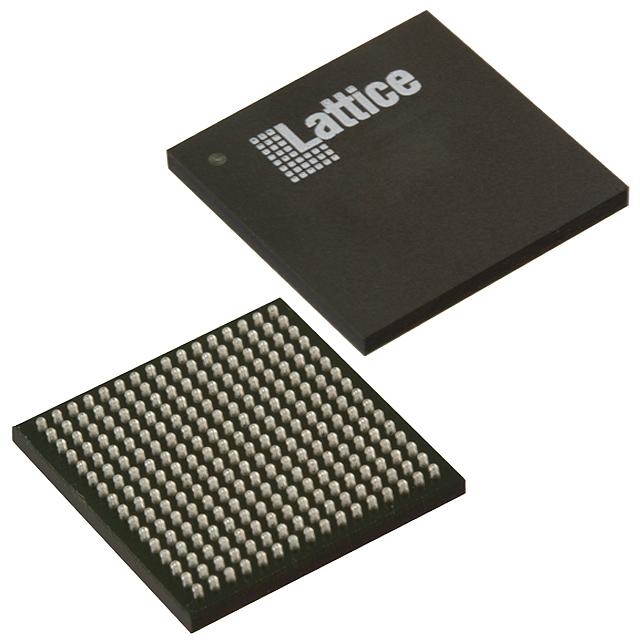
LFD2NX-40-8BG256I
LFD2NX-40-8BG256I ECAD Model
LFD2NX-40-8BG256I Attributes
| Type | Description | Select |
|---|---|---|
| Mfr | Lattice Semiconductor Corporation | |
| Series | Certus™-NX | |
| Package | Tray | |
| Number of LABs/CLBs | 9750 | |
| Number of Logic Elements/Cells | 39000 | |
| Total RAM Bits | 1548288 | |
| Number of I/O | 192 | |
| Voltage - Supply | 0.95V ~ 1.05V | |
| Mounting Type | Surface Mount | |
| Operating Temperature | -40°C ~ 100°C (TJ) | |
| Package / Case | 256-LFBGA | |
| Supplier Device Package | 256-CABGA (14x14) | |
| Base Product Number | LFD2NX-40 |
LFD2NX-40-8BG256I Datasheet Download
LFD2NX-40-8BG256I Overview
The LFD2NX-40-8BG256I is a Field Programmable Gate Array (FPGA) chip from Lattice Semiconductor. It is a low-cost, low-power, low-density FPGA designed for a wide range of applications. It features 8K logic elements, 256Kbits of embedded RAM, and 40 user-configurable I/O pins. The device is fabricated on a 0.35μm CMOS process and is capable of operating at core voltages ranging from 1.2V to 3.3V. It is also equipped with advanced power-saving features such as power-down mode, clock gating, and dynamic voltage scaling.
The LFD2NX-40-8BG256I is ideal for applications such as consumer electronics, automotive, industrial, and medical. It can be used to develop low-cost, low-power, and low-density designs for a wide range of applications. It can also be used for applications such as data acquisition, communications, motor control, and image processing. It is also suitable for applications that require high speed and low power consumption.
The LFD2NX-40-8BG256I comes with an on-board oscillator, programmable I/O, and built-in power-saving features. It also features a wide range of I/O standards such as LVTTL, LVCMOS, SSTL, and HSTL. It also supports a wide range of development tools such as Lattice Diamond, Lattice Radiant, and Lattice ispLEVER. The device is also supported by a wide range of third-party tools such as Synplicity and Mentor Graphics.
In summary, the LFD2NX-40-8BG256I is a low-cost, low-power, low-density FPGA designed for a wide range of applications. It features 8K logic elements, 256Kbits of embedded RAM, and 40 user-configurable I/O pins. It is suitable for applications such as consumer electronics, automotive, industrial, and medical. It is also supported by a wide range of development tools and third-party tools.
You May Also Be Interested In
3,021 In Stock
Pricing (USD)
| QTY | Unit Price | Ext Price |
|---|---|---|
| 1+ | $53.4539 | $53.4539 |
| 10+ | $52.8791 | $528.7912 |
| 100+ | $50.0053 | $5,000.5251 |
| 1000+ | $47.1314 | $23,565.6930 |
| 10000+ | $43.1080 | $43,107.9750 |
| The price is for reference only, please refer to the actual quotation! | ||