
Lattice Semiconductor Corporation
LFD2NX-40-7BG256C
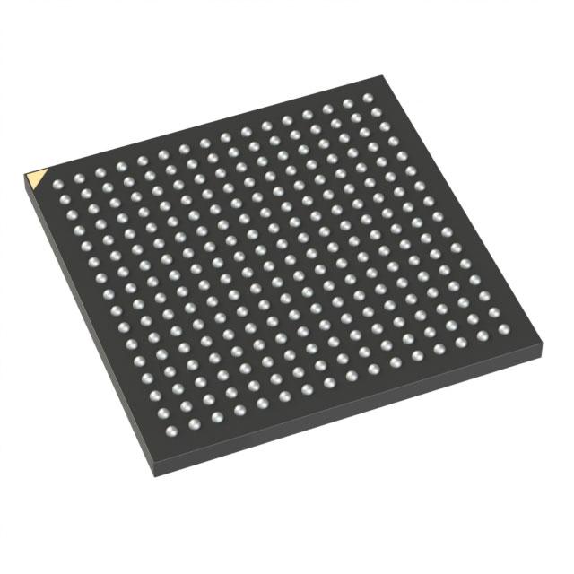
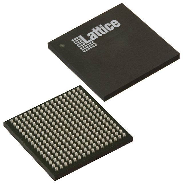
LFD2NX-40-7BG256C ECAD Model
LFD2NX-40-7BG256C Attributes
| Type | Description | Select |
|---|---|---|
| Mfr | Lattice Semiconductor Corporation | |
| Series | Certus™-NX | |
| Package | Tray | |
| Number of LABs/CLBs | 9750 | |
| Number of Logic Elements/Cells | 39000 | |
| Total RAM Bits | 1548288 | |
| Number of I/O | 192 | |
| Voltage - Supply | 0.95V ~ 1.05V | |
| Mounting Type | Surface Mount | |
| Operating Temperature | 0°C ~ 85°C (TJ) | |
| Package / Case | 256-LFBGA | |
| Supplier Device Package | 256-CABGA (14x14) | |
| Base Product Number | LFD2NX-40 |
LFD2NX-40-7BG256C Datasheet Download
LFD2NX-40-7BG256C Overview
The LFD2NX-40-7BG256C is a Field Programmable Gate Array (FPGA) chip model manufactured by Lattice Semiconductor. It is based on the company's low-power, low-cost Lattice FPGA architecture, which combines the low-power and low-cost benefits of a standard FPGA with the flexibility and scalability of a reconfigurable architecture. The chip has a total of 256Kbits of on-chip memory, with a total of 7 banks of 256Kbits each. It also features a total of 40 logic cells, with each logic cell having a dedicated programmable logic block. The chip is designed to be used in a wide range of applications, including embedded systems, data processing, and communications.
The chip is designed to be used in a variety of applications, including embedded systems, data processing, and communications. It is designed to be used in applications that require high levels of integration, low power consumption, and low cost. The chip also features a high-speed, low-power, embedded processor core, which enables high-speed data processing and communications. Additionally, the chip is designed to be used in applications that require a high degree of flexibility. The chip is also designed to be used in applications that require a high degree of scalability, allowing for the addition of additional logic blocks and memory banks.
The chip is also designed to be used in a variety of applications that require high levels of integration, low power consumption, and low cost. It is designed to be used in applications that require a high degree of flexibility, scalability, and performance. Additionally, the chip is designed to be used in applications that require a high degree of reliability and robustness. The chip is also designed to be used in applications that require high levels of security and encryption.
Overall, the LFD2NX-40-7BG256C is a powerful and flexible Field Programmable Gate Array (FPGA) chip model manufactured by Lattice Semiconductor. It features a total of 256Kbits of on-chip memory, with a total of 7 banks of 256Kbits each, and a total of 40 logic cells. The chip is designed to be used in a wide range of applications, including embedded systems, data processing, and communications. It is designed to provide high levels of integration, low power consumption, and low cost. Additionally, the chip is designed to be used in applications that require a high degree of flexibility, scalability, performance, reliability, robustness, security, and encryption.
You May Also Be Interested In
3,876 In Stock
Pricing (USD)
| QTY | Unit Price | Ext Price |
|---|---|---|
| 1+ | $42.2131 | $42.2131 |
| 10+ | $41.7592 | $417.5917 |
| 100+ | $39.4896 | $3,948.9648 |
| 1000+ | $37.2201 | $18,610.0640 |
| 10000+ | $34.0428 | $34,042.8000 |
| The price is for reference only, please refer to the actual quotation! | ||